4–24 Altera Corporation
Stratix Device Handbook, Volume 2 June 2006
Stratix & Stratix GX I/O Banks
Non-Voltage-Referenced Standards
Each Stratix I/O bank has its own VCCIO pins and supports only one
V
CCIO
, either 1.5, 1.8, 2.5 or 3.3 V. A Stratix I/O bank can simultaneously
support any number of input signals with different I/O standard
assignments, as shown in Table 4–5.
For output signals, a single I/O bank can only support non-voltage-
referenced output signals driving at the same voltage as V
CCIO
. A Stratix
I/O bank can only have one V
CCIO
value, so it can only drive out that one
value for non-voltage referenced signals. For example, an I/O bank with
a 2.5-V V
CCIO
setting can support 2.5-V LVTTL inputs and outputs,
HyperTransport technology inputs and outputs, and 3.3-V LVCMOS
inputs (not output or bidirectional pins).
1 If the output buffer overdrives the input buffer, you must turn
on the Allow voltage overdrive for LVTTL/LVCMOS option in
the Quartus II software. To see this option, click the Device &
Pin Options button in the Device page of the Settings dialog
box (Assignments menu). Then click the Pin Placement tab in
the Device & Pin Options dialog box.
Voltage-Referenced Standards
To accommodate voltage-referenced I/O standards, each Stratix I/O
bank supports multiple VREF pins feeding a common VREF bus. The
number of available VREF pins increases as device density increases. If
these pins are not used as VREF pins, they can not be used as generic I/O
pins.
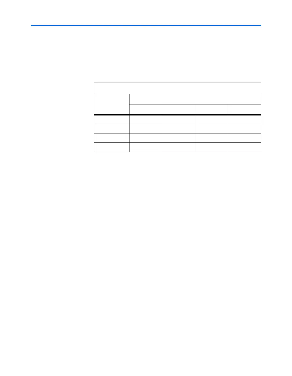
Table 4–5. Acceptable Input Levels for LVTTL/LVCMOS
Bank V
CCIO
Acceptable Input Levels
3.3 V 2.5 V 1.8 V 1.5 V
3.3 V vv
2.5 V vv
1.8 V v (2) v (2)
v
v (1)
1.5 V v (2) v (2)
vv
Notes to Ta b le 4 – 5 :
(1) Because the input signal will not drive to the rail, the input buffer does not
completely shut off, and the I/O current will be slightly higher than the default
value.
(2) These input values overdrive the input buffer, so the pin leakage current will be
slightly higher than the default value.