Altera Corporation 4–29
June 2006 Stratix Device Handbook, Volume 2
Selectable I/O Standards in Stratix & Stratix GX Devices
For more information on termination for voltage-referenced I/O
standards, see the Selectable I/O Standards in Stratix & Stratix GX Devices
chapter in the Stratix Device Handbook, Volume 2; or the Stratix GX Device
Handbook, Volume 2.
Differential I/O Standards
Differential I/O standards typically require a termination resistor
between the two signals at the receiver. The termination resistor must
match the differential load impedance of the bus. Stratix and Stratix GX
devices provide an optional differential termination on-chip resistor
when using LVDS.
See the High-Speed Differential I/O Interfaces in Stratix Devices chapter for
more information on differential I/O standards and their interfaces.
For differential I/O standards, I/O banks support differential
termination when V
CCIO
equals 3.3 V.
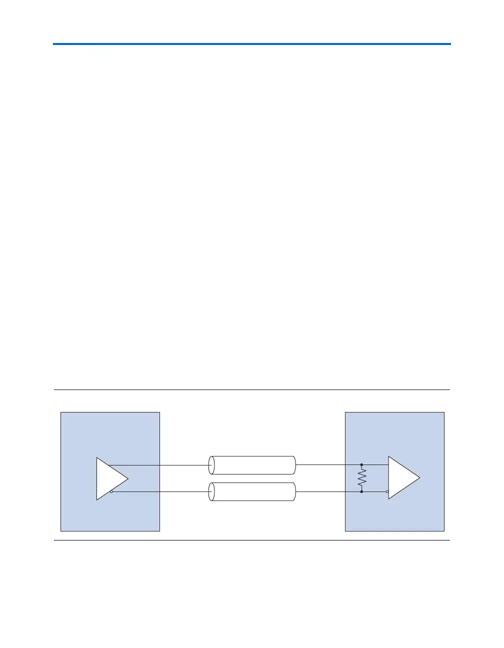
Differential Termination (R
D
)
Stratix devices support differential on-chip termination for source-
synchronous LVDS signaling. The differential termination resistors are
adjacent to the differential input buffers on the device. This placement
eliminates stub effects, improving the signal integrity of the serial link.
Using differential on-chip termination resistors also saves board space.
Figure 4–20 shows the differential termination connections for Stratix and
Stratix GX devices.
Figure 4–20. Differential Termination
Z
0
Z
0
Stratix LVDS
Receiver Buffer with
Differential On-Chip Termination
R
D
Differential
Transmitter