14–20 Altera Corporation
Stratix Device Handbook, Volume 2 January 2005
1.5-V Regulator Application Examples
Synchronous Switching Regulator Example
This example shows a worst-case scenario for power consumption where
the design uses all the LEs and RAM. Table 14–7 shows the design
requirements for 1.5-V design using a Cyclone EP1C12 FPGA.
Table 14–8 uses the checklist on page 14–9 to help select the appropriate
voltage regulator.
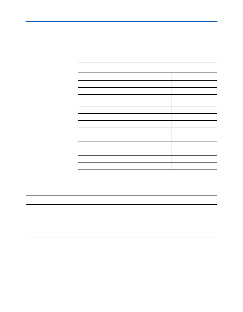
Table 14–7. Design Requirements for the Example EP1C12F324C
Design Requirement Value
Output voltage precision requirement ±5%
Supply voltages available on the board 3.3 V
Voltage supply output current available for this
section (I
IN, DC(MAX)
)
2 A
Variance of board supply (V
IN
) ±5%
f
MAX
150 MHz
Average tog
IO
12.5%
Average tog
LC
12.5%
Utilization 100%
Output and bidirectional pins 125
V
CCIO
supply level 3.3 V
V
CCINT
supply level 1.5 V
Efficiency ≥90%
Table 14–8. Voltage Regulator Selection Process for EP1C12F324C Design (Part 1 of 2)
Output voltage requirements V
OUT
= 1.5 V
Supply voltages V
IN
OR V
CC
= 3.3 V
Supply variance from Linear Technology data sheet Supply variance = ±5%
Estimated I
CCINT
Use Cyclone Power Calculator
I
CCINT
= 620 mA
Estimated I
CCIO
if regulator powers V
CCIO
Use Cyclone Power Calculator (not applicable in this example
because V
CCIO
= 3.3 V)
I
CCIO
= N/A
Total user-mode current consumption
I
CC
= I
CCINT
+ I
CCIO
I
CC
= 620 mA