9–10 Altera Corporation
Stratix Device Handbook, Volume 2 July 2005
Introduction
AC Timing Specifications
Figures 9–7 through 9–9 and Tables 9–4 through 9–6 illustrate the timing
characteristics of SFI-4 at the framer. Stratix and Stratix GX devices
support all the timing requirements needed to support transmitter and
receiver functions of a SFI-4 framer; only framer-related timing
specifications are applicable.
f For details on the timing specifications of LVDS I/O standards in Stratix
and Stratix GX devices, see the Stratix Device Family Data Sheet section of
the Stratix Device Handbook, Volume 1 and the High-Speed Differential I/O
Interfaces in Stratix Devices chapter or the Stratix GX Device Family Data
Sheet section of the Stratix GX Device Handbook, Volume 1 and the High-
Speed Differential I/O Interfaces in Stratix Devices chapter
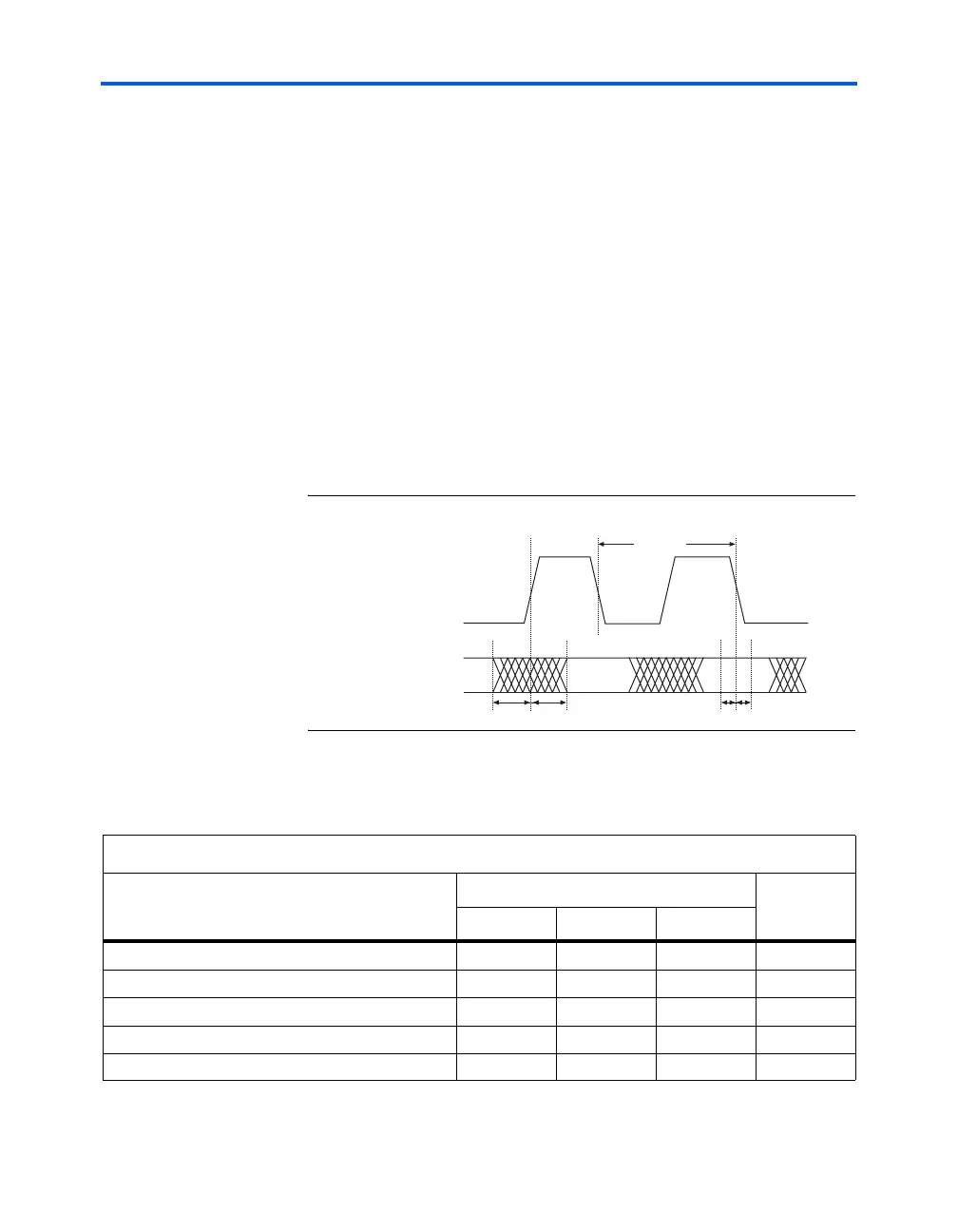
Figure 9–7 shows the timing diagram for the Stratix and Stratix GX
framer transmitter × 1 (622 MHz clock) mode.
Figure 9–7. Framer Transmitter × 1 (622 MHz Clock) Mode Timing Diagram
Table 9–4 lists the timing specifications for the SFI-4 framer transmitter in
× 1 (622 MHz clock) mode.
T
period
T
cq_pre
T
cq_post
T
setup
T
hold
Valid
Data
TX_DATA[15..0]
Table 9–4. SFI-4 Framer Transmitter × 1 (622 MHz Clock) Mode Timing Specifications
Parameter
Value
Unit
Min Typ Max
TX_CLK (T
period
)
1,608 ps
Data invalid window before the rising edge (T
cq_pre
)200ps
Data invalid window after the rising edge (T
cq_post
)200ps
TX_CLK duty cycle
40 60 %
Framer transmitter channel-to-channel skew 200 ps