5–2 Altera Corporation
Stratix Device Handbook, Volume 2 July 2005
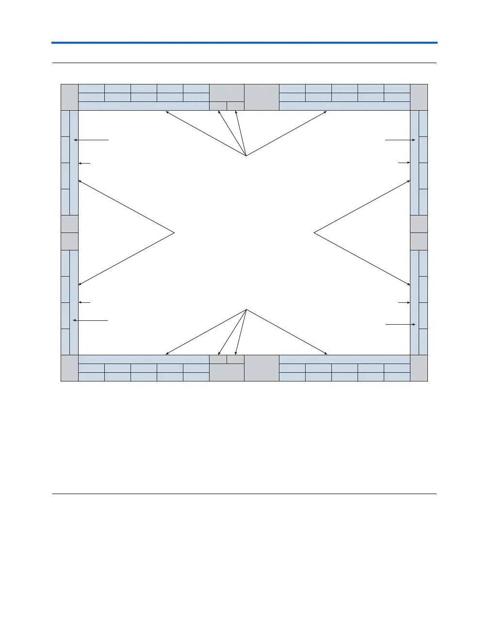
Stratix I/O Banks
Figure 5–1. Stratix I/O Banks Notes (1), (2), (3)
Notes to Figure 5–1:
(1) Figure 5–1 is a top view of the Stratix silicon die, which corresponds to a top-down view of non-flip-chip packages
and a bottom-up view of flip-chip packages.
(2) Figure 5–1 is a graphic representation only. See the pin list and the Quartus II software for exact locations.
(3) Banks 9 through 12 are enhanced PLL external clock output banks.
(4) If the high-speed differential I/O pins are not used for high-speed differential signaling, they can support all of the
I/O standards except HSTL Class I and II, GTL, SSTL-18 Class II, PCI, PCI-X 1.0, and AGP 1× /2× .
(5) See “Differential Pad Placement Guidelines” on page 4–30. You can only place single-ended output/bidirectional
pads five or more pads away from a differential pad. Use the Show Pads view in the Quartus II Floorplan Editor to
locate these pads. The Quartus II software gives an error message for illegal output or bidirectional pin placement
next to a high-speed differential I/O pin.
Stratix Differential I/O Standards
Stratix devices provide a multi-protocol interface that allows
communication between a variety of I/O standards, including LVDS,
HyperTransport technology, LVPECL, PCML, HSTL Class I and II, and
LVDS, LVPECL, 3.3-V PCML,
and HyperTransport I/O Block
and Regular I/O Pins (4)
LVDS, LVPECL, 3.3-V PCML,
and HyperTransport I/O Block
and Regular I/O Pins (4)
I/O Banks 3, 4, 9 & 10 Su
pport
All Single-Ended I/O Standards
I/O Banks 7, 8, 11 & 12 Support
All Single-Ended I/O Standards
I/O Banks 1, 2, 5, and 6 Support All
Single-Ended I/O Standards Except
Differential HSTL Output C
locks,
Differential SSTL-2 Output Clocks,
HSTL Class II, GTL, SSTL-18 Class II,
PCI, PCI-X 1.0, and AGP 1×/2×
DQS9T DQS8T DQS7T DQS6T DQS5T DQS4T DQS3T DQS2T DQS1T DQS0T
PLL5
VREF1B3 VREF2B3 VREF3B3 VREF4B3 VREF5B3 VREF1B4 VREF2B4 VREF3B4 VREF4B4 VREF5B4
VREF5B8 VREF4B8 VREF3B8 VREF2B8 VREF1B8 VREF5B7 VREF4B7 VREF3B7 VREF2B7 VREF1B7
PLL6
DQS9B DQS8B DQS7B DQS6B DQS5B DQS4B DQS3B DQS2B DQS1B DQS0B
910
VREF1B2 VREF2B2 VREF3B2 VREF4B2VREF1B1 VREF2B1 VREF3B1 VREF4B1
VREF4B6 VREF3B6 VREF2B6 VREF1B6 VREF4B5 VREF3B5 VREF2B5 VREF1B5
Bank 5Bank 6
PLL3
PLL4PLL1
PLL2
Bank 1
Bank 2
Bank 3 Bank 4
11 12Bank 8 Bank 7
LVDS, LVPECL, 3.3-V PCML,
and HyperTransport I/O Block
and Regular I/O Pins (4)
LVDS, LVPECL, 3.3-V PCML,
and HyperTransport I/O Block
and Regular I/O Pins (4)
PLL7 PLL10
PLL8 PLL9
PLL12
PLL11
(5)
(5)
(5)
(5)