Altera Corporation 5–43
July 2005 Stratix Device Handbook, Volume 2
High-Speed Differential I/O Interfaces in Stratix Devices
SERDES Bypass DDR Differential Signaling Receiver Operation
The SERDES bypass differential signaling receiver uses the Stratix device
DDR input circuitry to receive high-speed serial data. The DDR input
circuitry consists of a pair of shift registers used to capture the high-speed
serial data, and a latch.
One register captures the data on the positive edge of the clock (generated
by PLL) and the other register captures the data on the negative edge of
the clock. Because the data captured on the negative edge is delayed by
one-half of the clock cycle, it is latched before it interfaces with the system
logic.
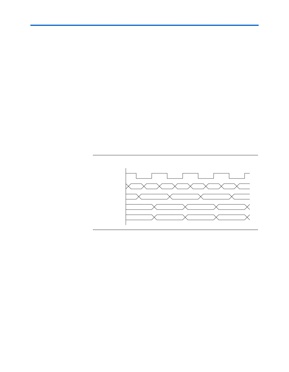
Figure 5–28 shows the DDR timing relationship between the incoming
serial data and the clock. In this example, the inclock signal is running
at half the speed of the incoming data. However, other combinations are
also possible. Figure 5–29 shows the DDR input and the other modules
used in a Flexible-LVDS receiver design to interface with the system logic.
Figure 5–28. ×2 Timing Relation between Incoming Serial Data & Clock
clock
datain
neg_reg_out
dataout_l
dataout_h
B0 A0 B1 A1 B2 A2 B3 A3
XX B0 B1 B2
XX B0 B1 B2
XX A0 A1 A2
B3