Altera Corporation 8–19
July 2005 Stratix Device Handbook, Volume 2
Implementing 10-Gigabit Ethernet Using Stratix & Stratix GX Devices
Timing
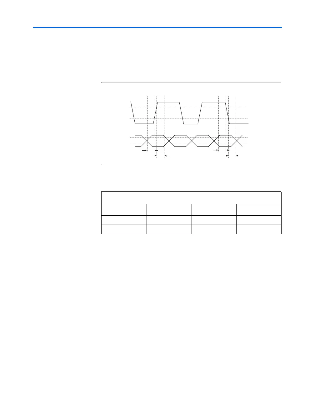
XGMII signals must meet the timing requirements shown in Figure 8–14.
Make all XGMII timing measurements at the driver output (shown in
Figure 8–14) and a capacitive load from all sources of 20 pF that are
specified relative to the V
IL
_AC(max) and V
IH
_AC(min) thresholds.
Figure 8–14. XGMII Timing Diagram
Table 8–8 shows the XGMII timing specifications.
Stratix and Stratix GX devices support DDR data with clock rates of up to
200 MHz, well above the XGMII clock rate of 156.25 MHz. For the HSTL
Class I I/O standard, Stratix and Stratix GX device I/O drivers provide a
1.0-V/ns slew rate at the input buffer of the receiving device.
XAUI
XAUI (pronounced Zowie) is located between the XGMII at the
reconciliation sublayer and the XGMII at the PHY layer. Figure 8–15
shows the location of XAUI. XAUI is designed to either extend or replace
XGMII in chip-to-chip applications of most Ethernet MAC to PHY
interconnects.
Table 8–8. XGMII Timing Specifications Note (1)
Symbol Driver Receiver Unit
T
setup
960 480 ps
T
hold
960 480 ps
Note to Ta b le 8 – 8 :
(1) The actual set-up and hold times will be made available after device
characterization is complete.
t
setup
t
hold
t
setup
t
hold
TX_CLK
RX_CLK
TXC, TXD,
RXC, RXD
V
IH
_AC(min)
V
IL
_AC(max)
V
IH
_AC(min)
V
IL
_AC(max)