5–40 Altera Corporation
Stratix Device Handbook, Volume 2 July 2005
Source-Synchronous Timing Budget
Output Timing
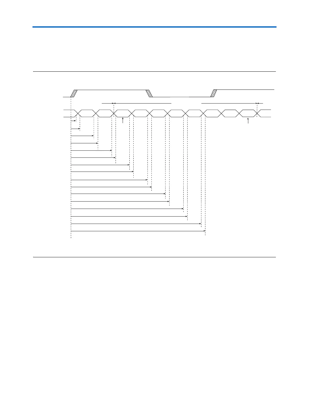
The output timing waveform in Figure 5–26 illustrates the relationship
between the output clock and the serial output data stream.
Figure 5–26. Output Timing Waveform Note (1)
Note to Figure 5–26:
(1) The timing specifications are referenced at a 250-mV differential voltage.
Receiver Skew Margin
Change in system environment, such as temperature, media (cable,
connector, or PCB) loading effect, a receiver's inherent setup and hold,
and internal skew, reduces the sampling window for the receiver. The
timing margin between receiver’s clock input and the data input
sampling window is known as RSKM. Figure 5–27 illustrates the
relationship between the parameter and the receiver’s sampling window.
Output Clock
(Differential
Signal)
Output Data
Previous Cycle Current Cycle
Next
Cycle
bit 2 bit 3 bit 4 bit 5 bit 6 bit 7bit 0 bit 1
MSB LSB
TPPos0 (min)
TPPos1 (min)
TPPos0 (max)
TPPos2 (min)
TPPos1 (max)
TPPos3 (min)
TPPos2 (max)
TPPos4 (min)
TPPos3 (max)
TPPos5
(min)
TPPos4 (max)
TPPos6 (min)
TPPos5 (max)
TPPos6 (max)
TPPos7 (min)
TPPos7 (max)