5–52 Altera Corporation
Stratix Device Handbook, Volume 2 July 2005
Software Support
Stratix devices can drive the PLL_LOCK signal to both output pins and
internal logic. As a result, you do not need a dedicated LOCK pin for your
PLLs. In addition, there is only one PLL_ENABLE pin that enables all the
PLLs on the device, including the fast PLLs. You must use either the
LVTTL or LVCMOS I/O standard with this pin.
Table 5–9 displays the LVDS pins in Stratix devices.
Fast PLLs
Each fast PLL features a multiplexed input path from a global or regional
clock net. A clock pin or an output from another PLL in the device can
drive the input path. The input clock for PLLs used to clock receiver the
rx_inclock port on the altlvds_rx megafunction must be driven by
a dedicated clock pin (CLK[3..0,8..11]) or the corner pins that clock the
corner PLLs (FPLL[10..7]CLK). EP1S10, EP1S20, and EP1S25 devices have
a total of four fast PLLs located in the center of both sides of the device
(see Figure 5–16 on page 5–23). EP1S30 and larger devices have two
additional fast PLLs per side at the top and bottom corners of the device.
As shown in Figure 5–17 on page 5–24, the corner fast PLL shares an I/O
bank with the closest center fast PLL (e.g., PLLs 1 and 7 share an I/O
bank). The maximum input clock frequency for enhanced PLLs is 684
MHz and 717 MHz for fast PLLs.
f For more information on Stratix PLLs, see the General-Purpose PLLs in
Stratix & Stratix GX Devices chapter.
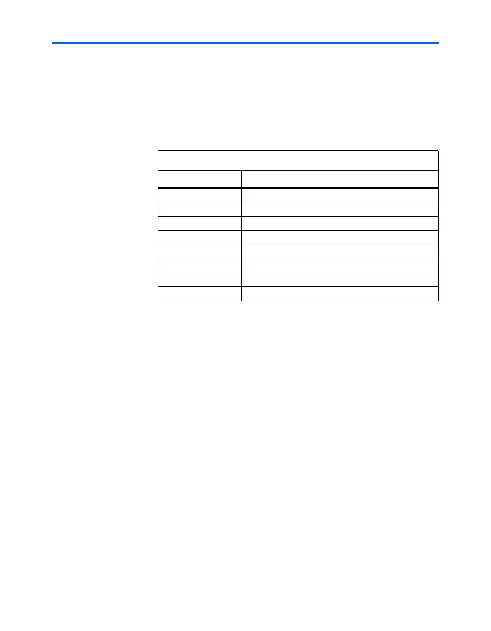
Table 5–9. LVDS Pin Names
Pin Names Functions
DIFFIO_TX#p
Transmitter positive data or output clock pin
DIFFIO_TX#n
Transmitter negative data or output clock pin
DIFFIO_RX#p
Receiver positive data pin
DIFFIO_RX#n
Receiver negative data pin
FPLLCLK#p
Positive input clock pin to the corner fast PLLs (1), (2)
FPLLCLK#n
Negative input clock pin to the corner fast PLLs (1), (2)
CLK#p
Positive input clock pin (2)
CLK#n
Negative input clock pin (2)
Notes to Ta b le 5 – 9 :
(1) The FPLLCLK pin-pair is only available in EP1S30, EP1S40, EP1S60, EP1S80
devices.
(2) Either a FPLLCLK pin or a CLK pin can drive the corner fast PLLs (PLL7, PLL8,
PLL9, and PLL10) when used for general purpose. CLK pins cannot drive these
fast PLLs in high-speed differential I/O mode.