5–46 Altera Corporation
Stratix Device Handbook, Volume 2 July 2005
Differential I/O Termination
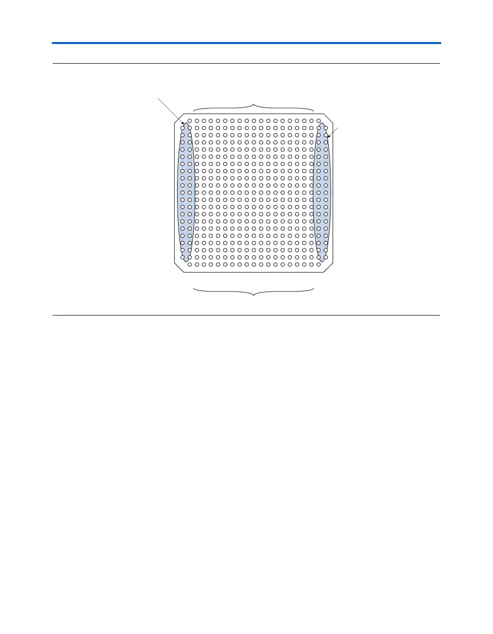
Figure 5–32. Differential I/O Pin Locations
Differential I/O
Termination
Stratix devices implement differential on-chip termination to reduce
reflections and maintain signal integrity. On-chip termination also
minimizes the number of external resistors required. This simplifies
board design and places the resistors closer to the package, eliminating
small stubs that can still lead to reflections.
R
D
Differential Termination
Stratix devices support differential on-chip termination for the LVDS I/O
standard. External termination is required on output pins for PCML
transmitters. HyperTransport, LVPECL, and LVDS receivers require
100 ohm termination at the input pins. Figure 5–33 shows the device with
differential termination for the LVDS I/O standard.
f For more information on differential on-chip termination technology, see
the Selectable I/O Standards in Stratix & Stratix GX Devices chapter.
U
T
R
P
N
M
L
K
J
H
G
F
E
D
C
B
A
V
W
Y
AA
21
20
19
18
17
16
15
14
13 9
10
11
12
8 6
75
4
3
2
1
Differential I/O Pins
(LVDS, LVPECL,
PCML, HyperTransport
Differential I/O Pins
(LVDS, LVPECL,
PCML, HyperTransport)
Regular I/O Pins
Regular I/O Pins