5–60 Altera Corporation
Stratix Device Handbook, Volume 2 July 2005
Software Support
When you span two I/O banks using cross-bank support, you can route
only two load enable signals total between the plls. When you enable
rx_data_align, you use both rxloadena and txloadena of a PLL.
That leaves no loadena for the second PLL.
The only way you can use the rx_data_align is if one of the following
is true:
■ The RX PLL is only clocking RX channels (no resources for TX)
■ If all channels can fit in one I/O bank
LVDS Receiver Block
You only need to enter the input clock frequency, deserialization factor,
and the input data rate to implement an LVDS receiver block. The
Quartus II software then automatically sets the clock boost (W) factor for
the receiver. In addition, you can also indicate the clock and data
alignment for the receiver or add the pll_enable, rx_data_align,
and rx_locked output ports. Table 5–15 explains the function of the
available ports in the LVDS receiver block.
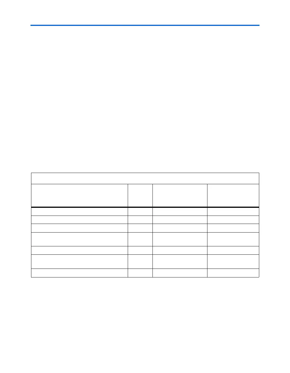
Table 5–15. LVDS Receiver Ports
Port Name Direction Function
Input Port
Source/Output Port
Destination
rx_in[number_of_channels - 1..0]
Input Input data channel Pin
rx_inclock
Input Reference input clock Pin or output from a PLL
rx_pll_enable
Input Enables fast PLL Pin (1), (2), (3)
rx_data_align
Input Control for the data
realignment circuitry
Pin or logic array (1),
(3), (4)
rx_locked
Output Fast PLL locked pin Pin or logic array (1), (3)
rx_out[Deserialization_factor *
number_of_channels -1..0]
Output De-serialized data Logic array
rx_outclock
Output Internal reference clock Logic array
Notes to Table 5–15:
(1) This is an optional port.
(2) Only one rx_pll_enable pin is necessary to enable all the PLLs in the device.
(3) This is a non-differential pin.
(4) See “Realignment Implementation” on page 5–28 for more information. For guaranteed performance and data
alignment, you must synchronize rx_data_align with rx_outclock.