Altera Corporation 5–65
July 2005 Stratix Device Handbook, Volume 2
High-Speed Differential I/O Interfaces in Stratix Devices
LVDS Transmitter Module
The Quartus II software calculates the inclock boost (W) factor for the
LVDS transmitter based on input data rate, input clock frequency, and
the deserialization factor. In addition to setting the data and clock
alignment, you can also set the outclock divide factor (B) for the
transmitter output clock and add the pll_enable, tx_locked, and
tx_coreclock ports. Table 5–16 explains the function of the available
ports in the LVDS transmitter block.
You can also use the altlvds MegaWizard Plug-In Manager to create an
LVDS transmitter block. The following sections explain the parameters
available in the Plug-In Manager when creating an LVDS transmitter
block.
Page 3 of the altlvds_tx MegaWizard Plug-In Manager
This section describes the parameters found on page 3 of the
altlvds_tx MegaWizard Plug-In Manager (see Figure 5–42).
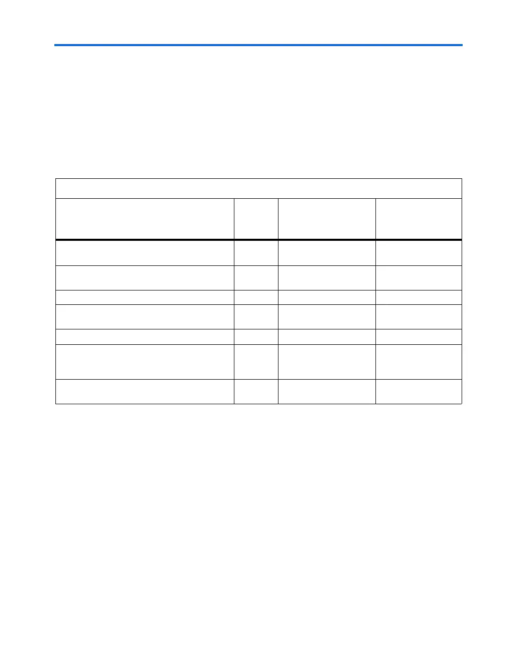
Table 5–16. LVDS Transmitter Ports
Port Name Direction Function
Input port
Source/Output port
Destination
tx_in[Deserialization_factor *
number_of_channels - 1..0]
Input Input data Logic array
tx_inclock
Input Reference input clock Pin or output clock
from a PLL
tx_pll_enable
Input Fast PLL enable Pin (1), (2), (3)
tx_out[number_of_channels - 1..0]
Output Serialized LVDS data
signal
Pin
tx_outclock
Output External reference clock Pin
tx_coreclock
Output Internal reference clock Pin, logic array, or
input clock to a fast
PLL (1)
tx_locked
Output Fast PLL locked pin Pin or logic array (1),
(2), (3)
Notes to Table 5–16:
(1) This is an optional port.
(2) Only one tx_pll_enable pin is necessary to enable all the PLLs in the device.
(3) This is a non-differential pin.