5–18 Altera Corporation
Stratix Device Handbook, Volume 2 July 2005
Differential I/O Interface & Fast PLLs
Clock Input & Fast PLL Output Relationship
Table 5–3 summarizes the PLL interface to the input clocks and the enable
signal (ENA). Table 5–4 summarizes the clock networks each fast PLL can
connect to across all Stratix family devices.
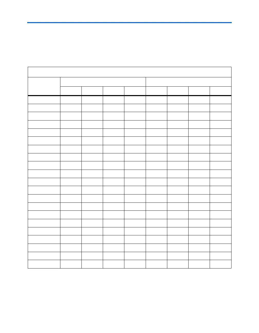
Table 5–3. Fast PLL Clock Inputs (Including Feedback Clocks) & Enables Note (1)
Input Pin
All Stratix Devices EP1S30 to EP1S80 Devices Only
PLL 1 PLL 2 PLL 3 PLL 4 PLL 7 PLL 8 PLL 9 PLL 10
CLK0 (2)
v
v (3)
CLK1
v
CLK2 (2)
v
v (3)
CLK3
v
CLK4
CLK5
CLK6
CLK7
CLK8
v
v (3)
CLK9 (2)
v
CLK10
v
v (3)
CLK11 (2)
v
CLK12
CLK13
CLK14
CLK15
ENA
vvvvvvvv
FPLL7CLK
v
FPLL8CLK
v
FPLL9CLK
v
FPLL10CLK
v
Notes to Ta b le 5 – 3 :
(1) PLLs 5, 6, 11, and 12 are not fast PLLs.
(2) Clock pins CLK0, CLK2, CLK9, CLK11, and pins FPLL[7..10]CLK do not support differential on-chip
termination.
(3) Either a FPLLCLK pin or a CLK pin can drive the corner fast PLLs (PLL7, PLL8, PLL9, and PLL10) when used for
general purpose. CLK pins cannot drive these fast PLLs in high-speed differential I/O mode.