2–14 Altera Corporation
Stratix Device Handbook, Volume 2 July 2005
Using TriMatrix Memory
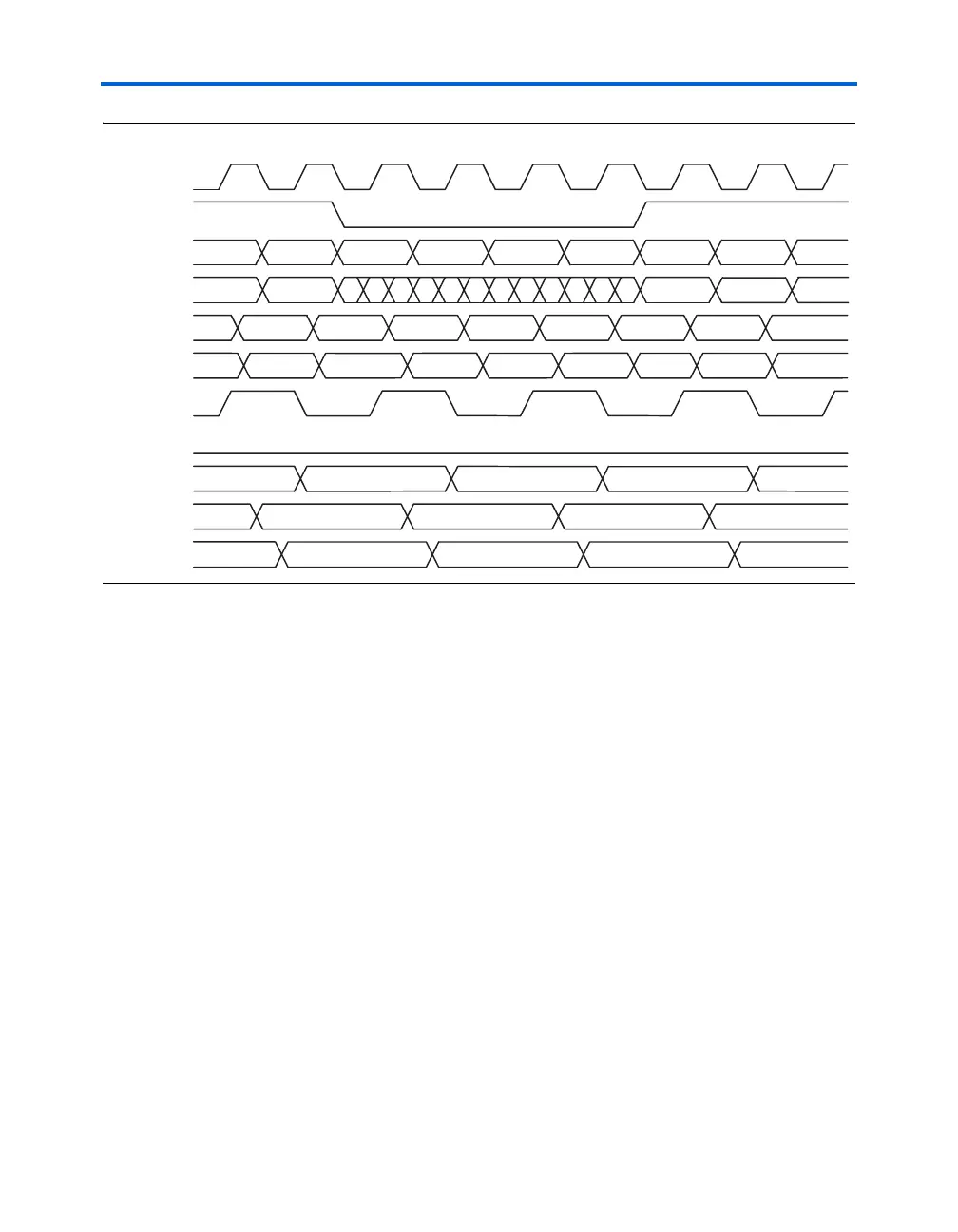
Figure 2–7. True Dual-Port Timing Waveforms
Implementing Shift-Register Mode
Embedded memory block configurations can implement shift registers
for digital signal processing (DSP) applications, such as finite impulse
response (FIR) filters, pseudo-random number generators, multi-channel
filtering, and auto-correlation and cross-correlation functions. These and
other DSP applications require local data storage, traditionally
implemented with standard flip-flops that can quickly consume many
logic cells for large shift registers. A more efficient alternative is to use
embedded memory as a shift register block, which saves logic cell and
routing resources and provides a more efficient implementation.
The size of a (w × m × n) shift register is determined by the input data
width (w), the length of the taps (m), and the number of taps (n). The size
of a (w × m × n) shift register must be less than or equal to the maximum
number of memory bits in the respective block: 576 bits for the M512
block and 4,608 bits for the M4K block. In addition, the size of w × n must
be less than or equal to the maximum width of the respective block: 18
bits for the M512 block and 36 bits for the M4K block. If a larger shift
register is required, the memory blocks can be cascaded together.
1 M-RAM blocks do not support the shift-register mode.
A_clk
A_wren
A_address
A_data_in
B_synch_data_out
an-1
an a0 a1 a2 a3 a4 a5
din-1 din din4 din5
B_clk
a6
din6
B_asynch_data_out
B_wren
B_address bn
b0
b1 b2 b3
doutn-2 doutn-1 doutn
doutn-1 doutn
dout0
A_synch_data_out
A_asynch_data_out
dout0
dout1
dout1
dout2
din-2 din-1
din
dout0 dout1 dout2 dout3
din4
din-1
din dout0
dout1 dout2
dout3
din4
din5