Altera Corporation 5–39
July 2005 Stratix Device Handbook, Volume 2
High-Speed Differential I/O Interfaces in Stratix Devices
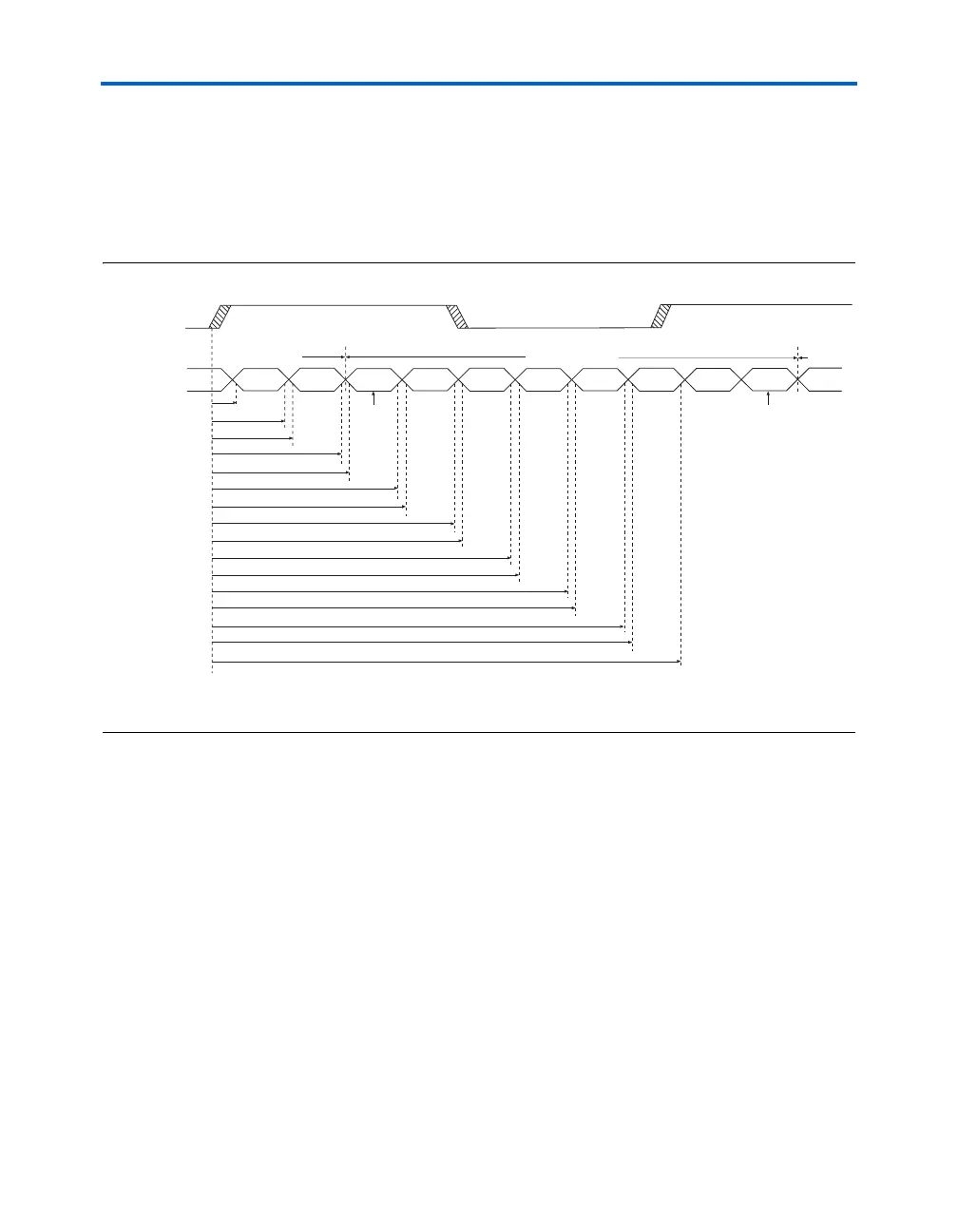
Input Timing Waveform
Figure 5–25 illustrates the essential operations and the timing
relationship between the clock cycle and the incoming serial data. For a
functional description of the SERDES, see “Principles of SERDES
Operation” on page 5–6.
Figure 5–25. Input Timing Waveform Note (1)
Note to Figure 5–25:
(1) The timing specifications are referenced at a 100-mV differential voltage.
Input Clock
(Differential
Signal)
Input Data
Previous Cycle
Current Cycle
Next
Cycle
bit 2 bit 3 bit 4 bit 5 bit 6 bit 7bit 0 bit 1
MSB LSB
t
sw0
(min)
t
sw1
(min)
t
sw0
(max)
t
sw2
(min)
t
sw1
(max)
t
sw3
(min)
t
sw2
(max)
t
sw4
(min)
t
sw3
(max)
t
sw5
(min)
t
sw4
(max)
t
sw6
(min)
t
sw5
(max)
t
sw6
(max)
t
sw7
(min)
t
sw7
(max)