11–36 Altera Corporation
Stratix Device Handbook, Volume 2 July 2005
Configuration Schemes
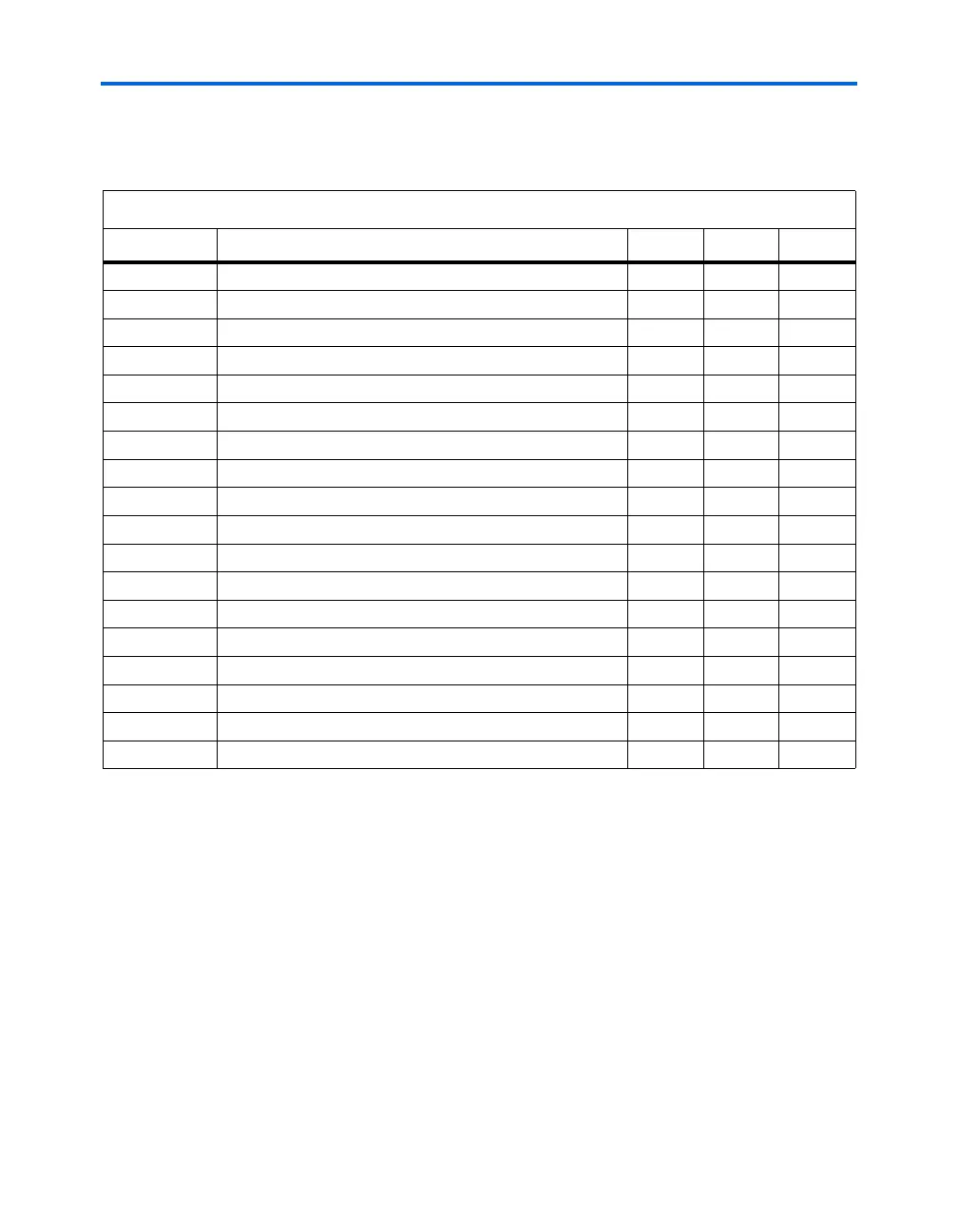
Table 11–10 defines the Stratix and Stratix GX timing parameters for PPA
configuration
f For information on how to create configuration and programming files
for this configuration scheme, see the Software Settings section in the
Configuration Handbook, Volume 2.
JTAG Programming & Configuration
The JTAG has developed a specification for boundary-scan testing. This
boundary-scan test (BST) architecture offers the capability to efficiently
test components on printed circuit boards (PCBs) with tight lead spacing.
The BST architecture can test pin connections without using physical test
Table 11–10. PPA Timing Parameters for Stratix & Stratix GX Devices
Symbol Parameter Min Max Units
t
CF2WS
nCONFIG high to first rising edge on nWS
40 µs
t
DSU
Data setup time before rising edge on nWS
10 ns
t
DH
Data hold time after rising edge on nWS
0ns
t
CSSU
Chip select setup time before rising edge on nWS
10 ns
t
CSH
Chip select hold time after rising edge on nWS
0ns
t
WSP
nWS low pulse width
15 ns
t
CFG
nCONFIG low pulse width
40 µs
t
WS2B
nWS rising edge to RDYnBSY low
20 ns
t
BUSY
RDYnBSY low pulse width
745ns
t
RDY2WS
RDYnBSY rising edge to nWS rising edge
15 ns
t
WS2RS
nWS rising edge to nRS falling edge
15 ns
t
RS2WS
nRS rising edge to nWS rising edge
15 ns
t
RSD7
nRS falling edge to DATA7 valid with RDYnBSY signal
20 ns
t
CD2UM
CONF_DONE high to user mode (1)
620µs
t
STATUS
nSTATUS low pulse width
10 40 (2) µs
t
CF2CD
nCONFIG low to CONF_DONE low
800 ns
t
CF2ST0
nCONFIG low to nSTATUS low
800 ns
t
CF2ST1
nCONFIG high to nSTATUS high
40 (2) µs
Notes to Table 11–10:
(1) The minimum and maximum numbers apply only if the internal oscillator is chosen as the clock source for starting
up the device. If the clock source is CLKUSR, multiply the clock period by 136 to obtain this value.
(2) This value is obtained if you do not delay configuration by extending the nstatus to low pulse width.
 Loading...