Altera Corporation 11–35
July 2005 Stratix Device Handbook, Volume 2
Configuring Stratix & Stratix GX Devices
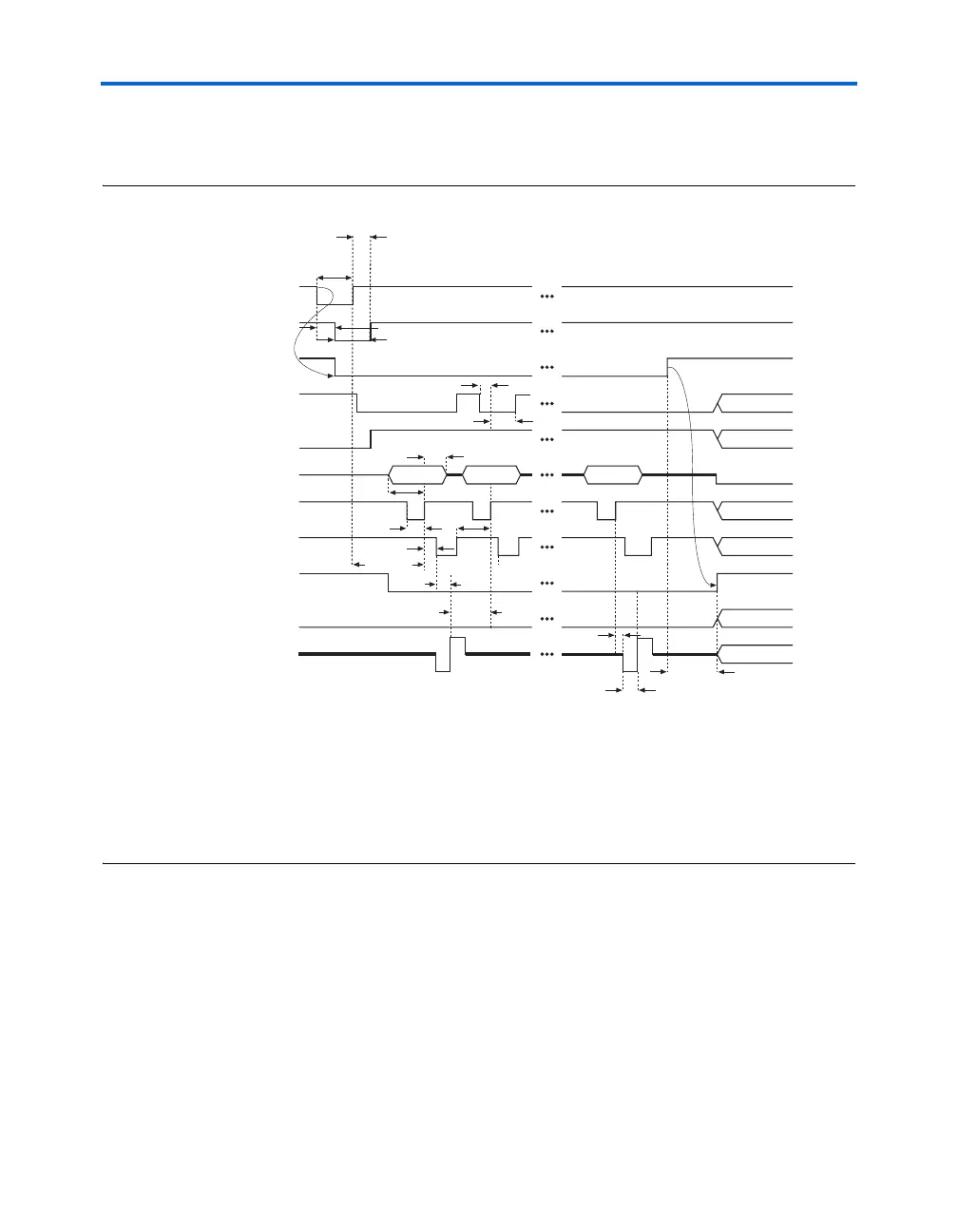
Figure 11–19 shows the Stratix and Stratix GX timing waveforms when
using strobed nRS and nWS signals.
Figure 11–19. PPA Timing Waveforms Using Strobed nRS & nWS Signals
Notes to Figure 11–19:
(1) The user can toggle nCS or CS during configuration if the design meets the specification for t
CSSU
, t
WSP
, and t
CSH
.
(2) Device I/O pins are in user mode.
(3) The DATA[7..0] pins are available as user I/Os after configuration and the state of theses pins depends on the
dual-purpose pin settings. Do not leave DATA[7..0] floating. If these pins are not used in user-mode, you should
drive them high or low, whichever is more convenient.
(4) DATA7 is a bidirectional pin. It represents an input for data input, but represents an output to show the status of
RDYnBSY.
Byte 0 Byte 1
Byte n
nCONFIG
nSTATUS
CONF_DONE
nCS (1)
CS (1)
DATA[7..0]
nWS
nRS
INIT_DONE
User I/O
DATA7/RDYnBSY (4)
t
CSSU
t
CFG
t
WSP
t
WS2RS
t
RSD7
t
RDY2WS
t
DH
t
BUSY
t
CSH
t
DSU
t
CF2WS
(2)
(2)
(3)
(2)
(2)
(2)
(2)
t
CD2UM
t
RS2WS
t
CF2ST1
t
CF2SCD
t
CF2ST0
t
STATUS
t
WS2RS
t
WS2B