Altera Corporation 5–11
July 2005 Stratix Device Handbook, Volume 2
High-Speed Differential I/O Interfaces in Stratix Devices
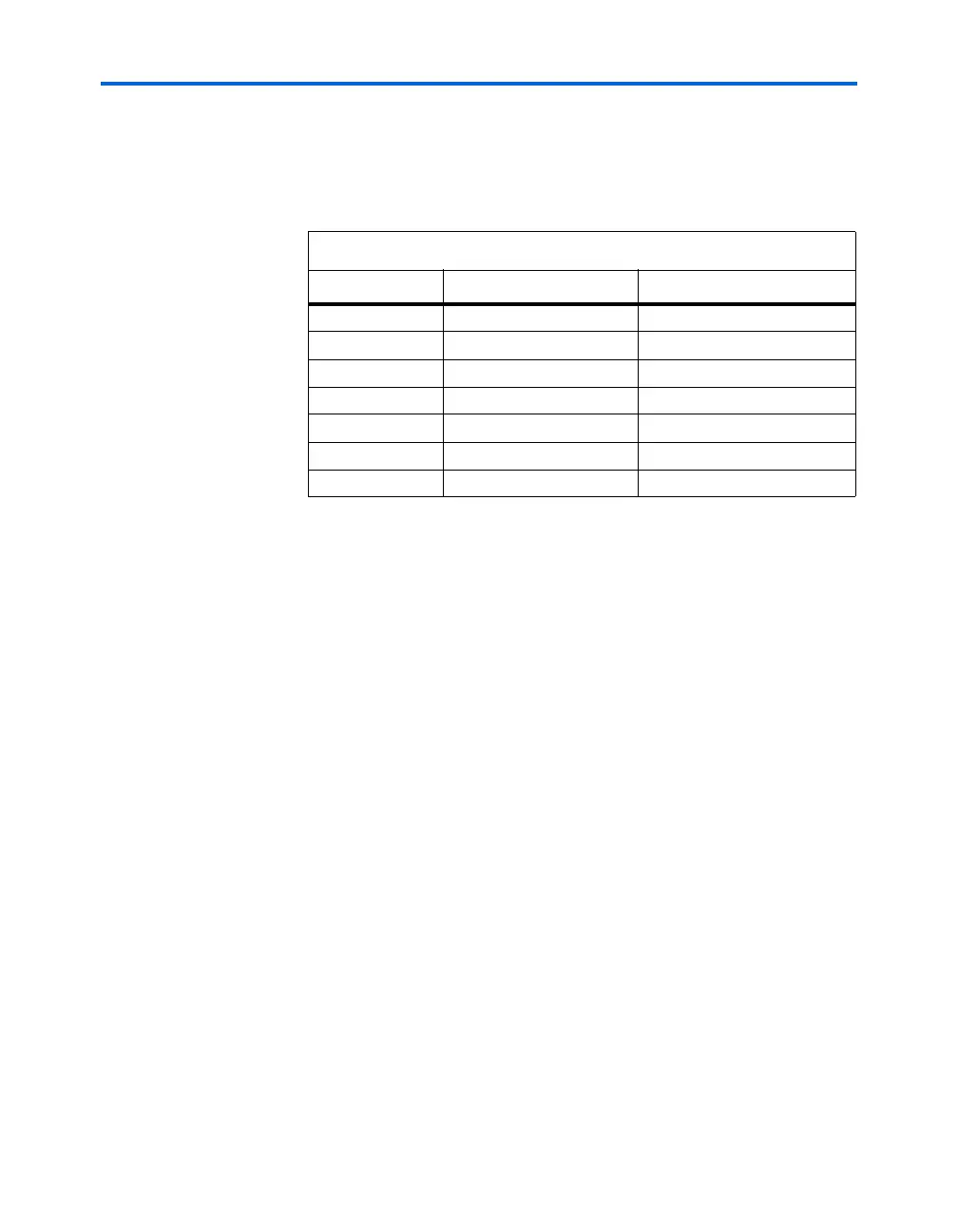
Table 5–2 shows the divided-down version of the high-frequency clock
and the selected serialization factor J (described in pervious sections). The
Quartus II software automatically generates the data input to the
additional transmitter data channel.
Center-Aligned Transmitter Clock Output
A negative-edge-triggered D flipflop (DFF) register is located between
the serial register of each data channel and its output buffer, as show in
Figure 5–7. The negative-edge-triggered DFF register is used when
center-aligned data is required. For center alignment, the DFF only shifts
the output from the channel used as the transmitter clock out. The
transmitter data channels bypass the negative-edge DFF. When you use
the DFF register, the data is transmitted at the negative edge of the
multiplied clock. This delays the transmitted clock output relative to the
data channels by half the multiplied clock cycle. This is used for
HyperTransport technology, but can also be used for any interface
requiring center alignment.
Table 5–2. Differential Transmitter Output Clock Division
J Data Input Output Clock Divided By (1)
4
1010
2
4
0011
4
8
10101010
2
8
00110011
4
8
11000011
8
10
1010101010
2
10
1110000011
10
Note to Ta b le 5 – 2 :
(1) This value is usually referred to as B.