5–10 Altera Corporation
Stratix Device Handbook, Volume 2 July 2005
Principles of SERDES Operation
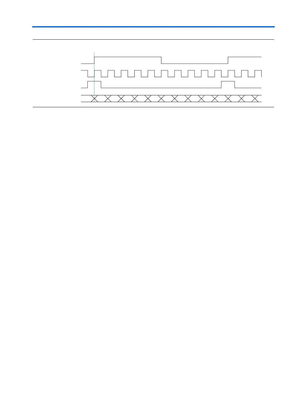
Figure 5–6. Transmitter Timing Diagram
Transmitter Clock Output
Different applications and protocols call for various clocking schemes.
Some applications require you to center-align the rising or falling clock
edge with the data. Other applications require a divide version of the
transmitted clock, or the clock and data to be at the same high-speed
frequency. The Stratix device transmitter clock output is versatile and
easily programmed for all such applications.
Stratix devices transmit data using the source-synchronous scheme,
where the clock is transmitted along with the serialized data to the
receiving device. Unlike APEX
TM
20KE and APEX II devices, Stratix
devices do not have a fixed transmitter clock output pin. The Altera
®
Quartus II software generates the transmitter clock output by using a fast
clock to drive a transmitter dataout channel. Therefore, you can place
the transmitter clock pair close to the data channels, reducing clock-to-
data skew and increasing system margins. This approach is more flexible,
as any channel can drive a clock, not just specially designated clock pins.
Divided-Down Transmitter Clock Output
You can divide down the high-frequency clock by 2, 4, 8, or 10, depending
on the system requirements. The various options allow Stratix devices to
accommodate many different types of protocols. The divided-down clock
is generated by an additional transmitting data channel.
TXLOADEN
Internal ×1 clock
Internal ×10 clock
Receiver
data input
n – 1 n – 0 9 8 7 6 5 4 3 2 1 0