Altera Corporation 11–3
July 2005 Stratix Device Handbook, Volume 2
Configuring Stratix & Stratix GX Devices
functionality while the system is in operation by reconfiguring the device.
You can also perform in-field upgrades by distributing a new
programming file to system users.
The following sections describe the MSEL[2..0], VCCSEL, PORSEL, and
nIO_PULLUP pins used in Stratix and Stratix GX device configuration.
MSEL[2..0] Pins
You can select a Stratix or Stratix GX device configuration scheme by
driving its MSEL2, MSEL1, and MSEL0 pins either high or low, as shown
in Table 11–2.
The MSEL[] pins can be tied to V
CCIO
of the I/O bank they reside in or
ground.
V
CCSEL
Pins
You can configure Stratix and Stratix GX devices using the 3.3-, 2.5-, 1.8-,
or 1.5-V LVTTL I/O standard on configuration and JTAG input pins.
VCCSEL is a dedicated input on Stratix and Stratix GX devices that selects
between 3.3-V/2.5-V input buffers and 1.8-V/1.5-V input buffers for
dedicated configuration input pins. A logic low supports 3.3-V/2.5-V
signaling, and a logic high supports 1.8-V/1.5-V signaling. A logic high
can also support 3.3-V/2.5-V signaling. VCCSEL affects the configuration
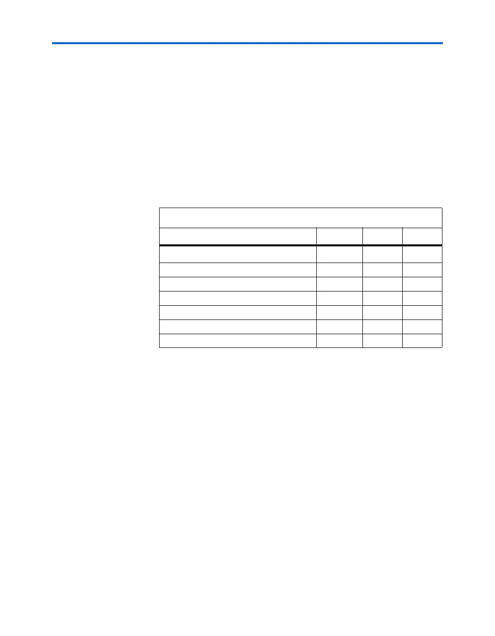
Table 11–2. Stratix & Stratix GX Device Configuration Schemes
Description MSEL2 MSEL1 MSEL0
FPP configuration
000
PPA configuration
001
PS configuration
010
Remote/local update FPP (1)
100
Remote/local update PPA (1)
101
Remote/local update PS (1)
110
JTAG-based configuration (3) (2) (2) (2)
Notes to Ta b le 11 – 2:
(1) These schemes require that you drive a secondary pin RUnLU to specify whether
to perform a remote update or local update.
(2) Do not leave MSEL pins floating. Connect them to V
CCIO
or GND. These pins
support the non-JTAG configuration scheme used in production. If only JTAG
configuration is used you should connect the MSEL pins to ground.
(3) JTAG-based configuration takes precedence over other configuration schemes,
which means the MSEL pins are ignored.