11–4 Altera Corporation
Stratix Device Handbook, Volume 2 July 2005
Device Configuration Overview
related I/O banks (3, 4, 7, and 8) where the following pins reside: TDI,
TMS, TCK, TRST, MSEL0, MSEL1, MSEL2, nCONFIG, nCE, DCLK, PLL_ENA,
CONF_DONE, nSTATUS. The VCCSEL pin can be pulled to 1.5, 1.8, 2.5, or
3.3-V for a logic high level. There is an internal 2.5-kΩ pull-down resistor
on VCCSEL. Therefore, if you are using a pull-up resister to pull up this
signal, you need to use a 1-kΩ resistor.
VCCSEL also sets the power-on-reset (POR) trip point for all the
configuration related I/O banks (3, 4, 7, and 8), ensuring that these I/O
banks have powered up to the appropriate voltage levels before
configuration begins. Upon power-up, the FPGA does not release
nSTATUS until V
CCINT
and all of the V
CCIO
s of the configuration I/O
banks are above their POR trip points. If you set VCCSEL to ground (logic
low), this sets the POR trip point for all configuration I/O banks to a
voltage consistent with 3.3-V/2.5-V signaling. When VCCSEL = 0, the
POR trip point for these I/O banks may be as high as 1.8 V. If V
CCIO
of any
of the configuration banks is set to 1.8 or 1.5 V, the voltage supplied to this
I/O bank(s) may never reach the POR trip point, which will not allow the
FPGA to begin configuration.
1 If the V
CCIO
of I/O banks 3, 4, 7, or 8 is set to 1.5 or 1.8 V and the
configuration signals used require 3.3-V or 2.5-V signaling you
should set VCCSEL to V
CC
(logic high) in order to lower the POR
trip point to enable successful configuration.
Table 11–3 shows how you should set the VCCSEL depending on the
V
CCIO
setting of the configuration I/O banks and your configuration
input signaling voltages.
The VCCSEL signal does not control any of the dual-purpose pins,
including the dual-purpose configuration pins, such as the DATA[7..0]
and PPA pins (nWS, nRS, CS, nCS, and RDYnBSY). During configuration,
these dual-purpose pins drive out voltage levels corresponding to the
V
CCIO
supply voltage that powers the I/O bank containing the pin. After
configuration, the dual-purpose pins inherit the I/O standards specified
in the design.
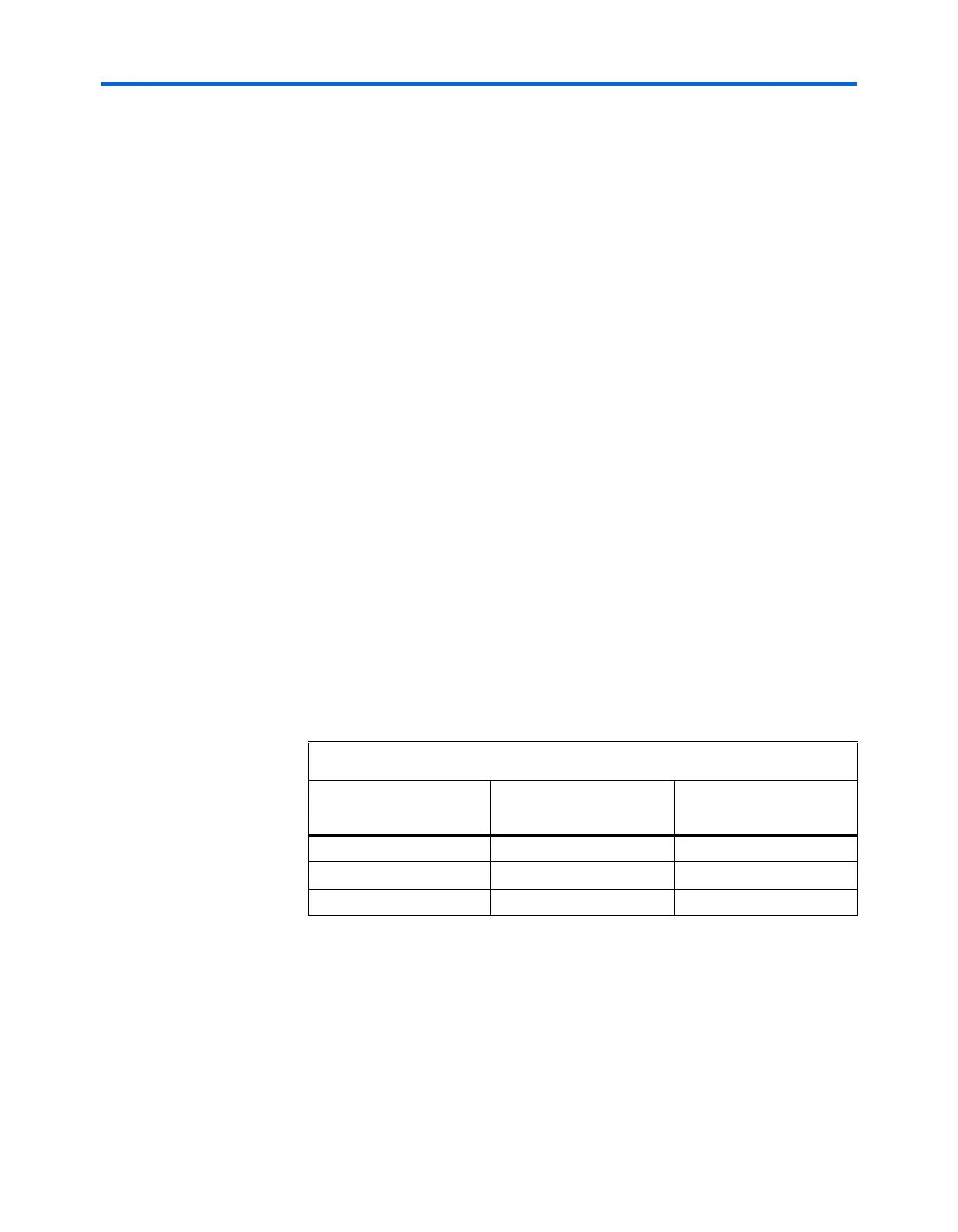
Table 11–3. VCCSEL Setting
V
CCIO
(banks 3,4,7,8)
Configuration Input
Signaling Voltage
V
CCSEL
3.3-V/2.5-V 3.3-V/2.5-V GND
1.8-V/1.5-V 3.3-V/2.5-V/1.8-V/1.5-V VCC
3.3-V/2.5-V 1.8-V/1.5-V Not Supported