Altera Corporation 14–21
January 2005 Stratix Device Handbook, Volume 2
Designing with 1.5-V Devices
Board Layout
Laying out a printed circuit board (PCB) properly is extremely important
in high-frequency (≥100 kHz) switching regulator designs. A poor PCB
layout results in increased EMI and ground bounce, which affects the
reliability of the voltage regulator by obscuring important voltage and
current feedback signals. Altera recommends using Gerber files ⎯pre-
designed layout files⎯supplied by the regulator vendor for your board
layout.
If you cannot use the supplied layout files, contact the voltage regulator
vendor for help on re-designing the board to fit your design requirements
while maintaining the proper functionality.
Altera recommends that you use separate layers for signals, the ground
plane, and voltage supply planes. You can support separate layers by
using multi-layer PCBs, assuming you are using two signal layers.
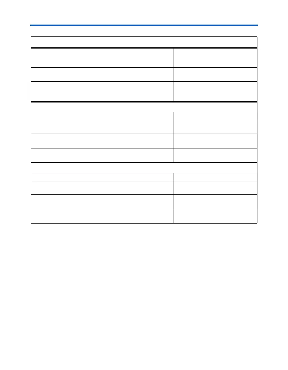
EP1C12 maximum power-up current requirement
See Power Consumption section of the Cyclone FPGA Family
Data Sheet for other densities
I
PUC(MAX)
= 900 mA
Maximum output current required
Compare I
CC
with I
PUC(MAX)
I
OUT(MAX)
= 900 mA
Voltage regulator selection
See Linear Technology LTC 1649 data sheet
See Intersil (Elantec) EL7562C data sheet
LTC1649 I
OUT(MAX)
=
EL7562C I
OUT(MAX)
=
15 A
2 A
LTC1649
Nominal efficiency (η) Nominal efficiency (η) = > 90%
Line and load regulation
Line regulation + load regulation = (0.17 mV + 7 mV)/ 1.5 V × 100%
Line and Load
Regulation = 0.478% < 5%
Minimum input voltage (V
IN(MIN)
)
(V
IN(MIN)
) = V
IN
(1 – ΔV
IN
) = 3.3V(1 – 0.05)
(V
IN(MIN)
) = 3.135 V
Maximum input current
I
IN, DC(MAX)
= (V
OUT
× I
OUT(MAX)
)/(η × V
IN(MIN)
)
I
IN, DC(MAX)
= 478 mA < 2 A
EL7562C
Nominal efficiency (η) Nominal efficiency (η) = > 95%
Line and load regulation
Line regulation + load regulation = (0.17 mV + 7 mV)/ 1.5 V × 100%
Line and Load
Regulation = 0.5% < 5%
Minimum input voltage (V
IN(MIN)
)
(V
IN(MIN)
) = V
IN
(1 – ΔV
IN
) = 3.3V(1 – 0.05)
(V
IN(MIN)
) = 3.135 V
Maximum input current
I
IN, DC(MAX)
= (V
OUT
× I
OUT(MAX)
)/(η × V
IN(MIN)
)
I
IN, DC(MAX)
= 453 mA < 2 A
Table 14–8. Voltage Regulator Selection Process for EP1C12F324C Design (Part 2 of 2)