8–18 Altera Corporation
Stratix Device Handbook, Volume 2 July 2005
Interfaces
V HSTL I/O pins for data and control and 2 clock pins for the transmitter
and receiver clocks. Each XGMII core also needs two PLLs (one for each
direction).
Reduced System Noise
The output buffer of each Stratix and Stratix GX device I/O pin has a
programmable drive strength control for certain I/O standards. The 1.5-
V HSTL Class I standard supports the minimum setting, which is the
lowest drive strength that guarantees I
OH
and I
OL
of the standard. Using
minimum settings provides signal slew rate control to reduce system
noise and signal overshoot.
f For more information on I
OH
and I
OL
values, see Operating Conditions in
the DC & Switching Characteristics chapter of the Stratix Device Handbook,
Volume 1 or Operating Conditions in the DC & Switching Characteristics
chapter of the Stratix GX Device Handbook, Volume 1.
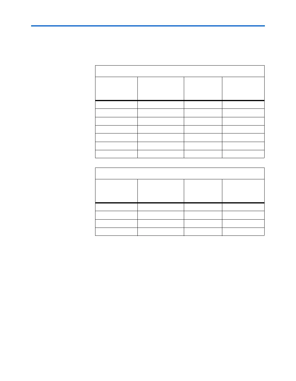
Table 8–6. Stratix XGMII Core Support
Stratix Device
Number of 1.5-V
HSTL Class I I/O
Pins
Number of Fast
& Enhanced
PLLs
Number of XGMII
Interfaces
EP1S10 410 6 3
EP1S20 570 6 3
EP1S25 690 6 3
EP1S30 718 10 5
EP1S40 814 12 6
EP1S60 1,014 12 6
EP1S80 1,195 12 6
Table 8–7. Stratix GX XGMII Core Support
Stratix Device
Number of 1.5-V
HSTL Class I I/O
Pins
Number of Fast
& Enhanced
PLLs
Number of XGMII
Interfaces
EP1SGX10 C, D 226 4 2
EP1SGX25 C 253 4 2
EP1SGX25 D, F 370 4 2
EP1SGX40 D, G 430 8 4