Altera Corporation 3–3
June 2006 Stratix Device Handbook, Volume 2
External Memory Interfaces in Stratix & Stratix GX Devices
Read & Write Operations
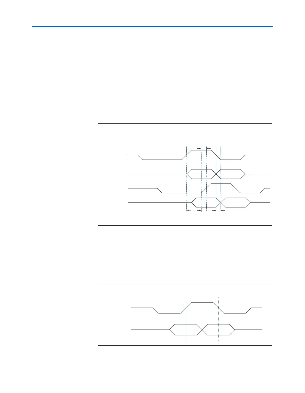
When reading from the DDR SDRAM, the DQS signal coming into the
Stratix and Stratix GX device is edge-aligned with the DQ pins. The
dedicated circuitry center-aligns the DQS signal with respect to the DQ
signals and the shifted DQS bus drives the clock input of the DDR input
registers. The DDR input registers bring the data from the DQ signals to
the device. The system clock clocks the DQS output enable and output
paths. The -90° shifted clock clocks the DQ output enable and output
paths. Figure 3–1 shows an example of the DQ and DQS relationship
during a burst-of-two read. It shows where the DQS signal is
center-aligned in the IOE.
Figure 3–1. Example of Where a DQS Signal is Center-Aligned in the IOE
When writing to the DDR SDRAM, the DQS signal must be center-
aligned with the DQ pins. Two PLL outputs are needed to generate the
DQS signal and to clock the DQ pins. The DQS are clocked by the 0°
phase-shift PLL output, while the DQ pins are clocked by the -90° phase-
shifted PLL output. Figure 3–2 shows the DQS and DQ relationship
during a DDR SDRAM burst-of-two write.
Figure 3–2. DQ & DQS Relationship During a Burst-of-Two Write
DQS at DQ
IOE registers
DQS at
FPGA Pin
DQ at DQ
IOE registers
DQ at
FPGA Pin
Pin to register
delay
Pin to register
delay
90 degree shift
Preamble
Postamble
DQS at
FPGA Pin
DQ at
FPGA Pin