Altera Corporation 5–15
July 2005 Stratix Device Handbook, Volume 2
High-Speed Differential I/O Interfaces in Stratix Devices
automatically assigns a seventeenth channel as the transmitter clock
output. You can edge- or center-align the transmitter clock output by
selecting the default PLL phase or selecting the 90° phase of the PLL
output. On the receiver side, the clock signal is connected to the receiver
PLL's clock input, and you can assign identical clock-to-data alignment.
The multiplication factor W is calculated automatically. The data rate is
dividing by the input clock frequency to calculate the W factor. The
deserialization factor J may be 4, 7, 8, or 10.
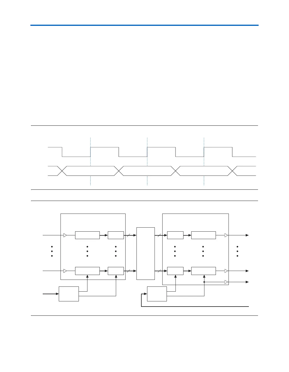
Figure 5–11 shows an SDR clock-to-data timing relationship, with clock
center aligned with respect to data. Figure 5–12 shows the connection
between the receiver and transmitter circuits.
Figure 5–11. SDR Clock-to-Data Relationship
Figure 5–12. SDR Receiver & Transmitter Circuit Connection
XX B0 B1 B2 B3
inclock
SDR
Serial-to-Parallel
Register
Parallel
Register
rx_d[0]
Channel
0
8
Parallel-to-Serial
Register
Parallel
Register
tx_d[0]
Channel
0
8
Serial-to-Parallel
Register
Parallel
Register
rx_d[15]
Channel
15
8
Parallel-to-Serial
Register
Parallel
Register
tx_d[15]
Channel
15
txclk_out
Channel
16
8
LVDS PLL LVDS PLL
txloaden
rxloaden input clock ×
W
input clock ×
W
txclk_in
624 MHz
624 MHz
Stratix
Logic
Array
Stratix SERDES SDR TransmitterStratix SERDES SDR Receiver
data rate = 624 Mbps
data rate = 624 Mbps
rxclk
624 MHz