Altera Corporation 1–51
July 2005 Stratix Device Handbook, Volume 2
General-Purpose PLLs in Stratix & Stratix GX Devices
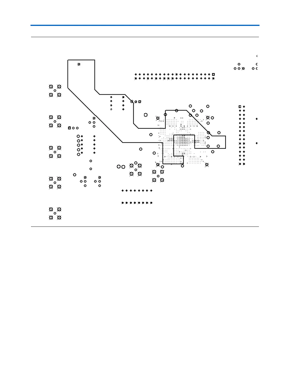
Figure 1–23. V
CCINT
Plane Partitioned for V
CCA
Island
Thick V
CCA
Trace
Because of board constraints, you might not be able to partition a V
CCA
island. Instead, run a thick trace from the power supply to each V
CCA
pin.
The traces should be at least 20 mils thick.
In each of these three cases, you should filter each V
CCA
pin with a
decoupling circuit shown in Figure 1–24. Place a ferrite bead that exhibits
high impedance at frequencies of 50 MHz or higher and a 10-μF tantalum
parallel capacitor where the power enters the board. Decouple each V
CCA
pin with a 0.1-μF and 0.001-μF parallel combination of ceramic capacitors
located as close as possible to the Stratix or Stratix GX device. You can
connect the GNDA pins directly to the same ground plane as the device’s
digital ground.