8–42 Chapter 8: Configuration and Remote System Upgrades in Cyclone IV Devices
Configuration
Cyclone IV Device Handbook, May 2013 Altera Corporation
Volume 1
To e nsu re that
DCLK
and
DATA[0]
are not left floating at the end of the configuration,
the MAX II device must drive them either high or low, whichever is convenient on
your board. The
DATA[0]
pin is available as a user I/O pin after configuration. When
you choose the FPP scheme in the Quartus II software, the
DATA[0]
pin is tri-stated by
default in user mode and must be driven by the external host device. To change this
default option in the Quartus II software, select the Dual-Purpose Pins tab of the
Device and Pin Options dialog box.
The
DCLK
speed must be below the specified system frequency to ensure correct
configuration. No maximum
DCLK
period exists, which means you can pause
configuration by halting
DCLK
for an indefinite amount of time.
The external host device can also monitor the
CONF_DONE
and
INIT_DONE
pins to ensure
successful configuration. The
CONF_DONE
pin must be monitored by the external device
to detect errors and to determine when programming is complete. If all configuration
data is sent, but
CONF_DONE
or
INIT_DONE
has not gone high, the external device must
reconfigure the target device.
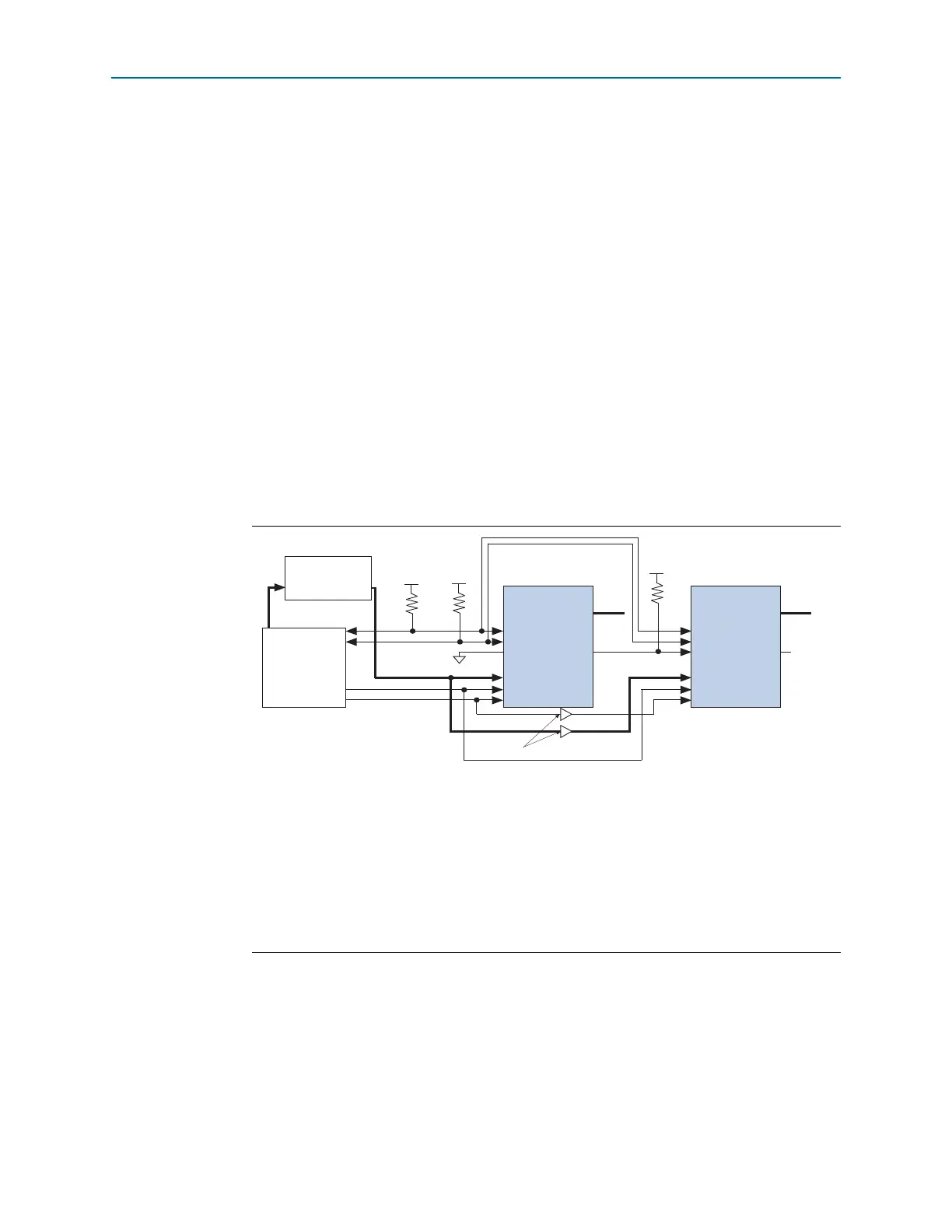
Figure 8–20 shows how to configure multiple devices with a MAX II device. This
circuit is similar to the FPP configuration circuit for a single device, except the
Cyclone IV devices are cascaded for multi-device configuration.
After the first device completes configuration in a multi-device configuration chain,
its
nCEO
pin drives low to activate the
nCE
pin of the second device, which prompts the
second device to begin configuration. The second device in the chain begins
configuration in one clock cycle; therefore, the transfer of data destinations is
transparent to the MAX II device. All other configuration pins (
nCONFIG
,
nSTATUS
,
Figure 8–20. Multi-Device FPP Configuration Using an External Host
Notes to Figure 8–20:
(1) The pull-up resistor must be connected to a supply that provides an acceptable input signal for all devices in the
chain. V
CC
must be high enough to meet the V
IH
specification of the I/O on the device and the external host.
(2) Connect the pull-up resistor to the V
CCIO
supply voltage of the I/O bank in which the
nCE
pin resides.
(3) The
nCEO
pin is left unconnected or used as a user I/O pin when it does not feed the
nCE
pin of another device.
(4) The
MSEL
pin settings vary for different configuration voltage standards and POR time. To connect the
MSEL
pins,
refer to Table 8–4 on page 8–8 and Table 8–5 on page 8–9. Connect the
MSEL
pins directly to V
CCA
or GND.
(5) All I/O inputs must maintain a maximum AC voltage of 4.1 V.
DATA[7..0]
and
DCLK
must fit the maximum overshoot
outlined in Equation 8–1 on page 8–5.
External Host
(MAX II Device or
Microprocessor)
Memory
ADDR
Cyclone IV Device 1
nSTATUS
CONF_DONE
10 k
nCE
nCEO
DATA[7..0]
GND
V
CCIO
(1)
V
CCIO
(1)
10 k
MSEL[3..0]
DATA[7..0]
(5)
nCONFIG
DCLK
(5)
nSTATUS
CONF_DONE
nCE
nCEO
N.C. (3
DATA[7..0]
(5)
nCONFIG
DCLK
(5)
V
CCIO (2)
10 k
Cyclone IV Device 2
(4)
(4)
Buffers (5)
MSEL[3..0]