3–18 Altera Corporation
Stratix Device Handbook, Volume 2 June 2006
DDR Memory Support Overview
To generate the correct phase shift, you must provide a clock signal of the
same frequency as the DQS signal to the DQS phase-shift circuitry. Any
of the CLK[15..12]p clock pins can feed the phase circuitry on the top
of the device (I/O banks 3 and 4) and any of the CLK[7..4]p clock pins
can feed the phase circuitry on the bottom of the device (I/O banks 7
and 8). Both the top and bottom phase-shift circuits need unique clock
pins for the reference clock. You cannot use any internal clock sources to
feed the phase-shift circuitry, but you can route internal clock sources
off-chip and then back into one of the allowable clock input pins.
DLL
The DQS phase-shift circuitry uses a DLL to dynamically measure the
clock period needed by the DQS pin (see Figure 3–9). The DQS
phase-shift circuitry then uses the clock period to generate the correct
phase shift. The DLL in the Stratix and Stratix GX devices DQS phase-
shift circuitry can operate between 100 and 200 MHz. The phase-shift
circuitry needs a maximum of 256 clock cycles to calculate the correct
phase shift. Data sent during these clock cycles may not be properly
captured.
1 You can still use the DQS phase-shift circuitry for DDR SDRAM
interfaces that are less than 100 MHz. The DQS signal is shifted
by about 2.5 ns. This shifted DQS signal is not in the center of the
DQ signals, but it is shifted enough to capture the correct data in
this low-frequency application.
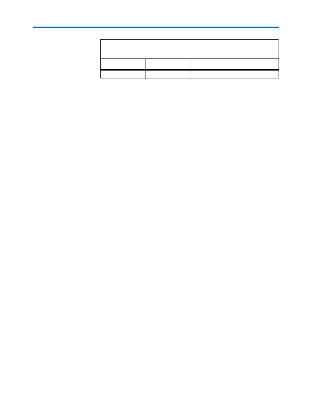
-8 1.293 1.635 ns
Note to Ta b le 3 – 4 :
(1) These are reported by Quartus II version 4.0. Check the latest version of the
Quartus II software for the most current information.
Table 3–4. Quartus II Reported Number on the DQS Path to the
IOE Note (1)
Speed Grade DQ2IOE DQS2IOE Unit