Altera Corporation 3–17
June 2006 Stratix Device Handbook, Volume 2
External Memory Interfaces in Stratix & Stratix GX Devices
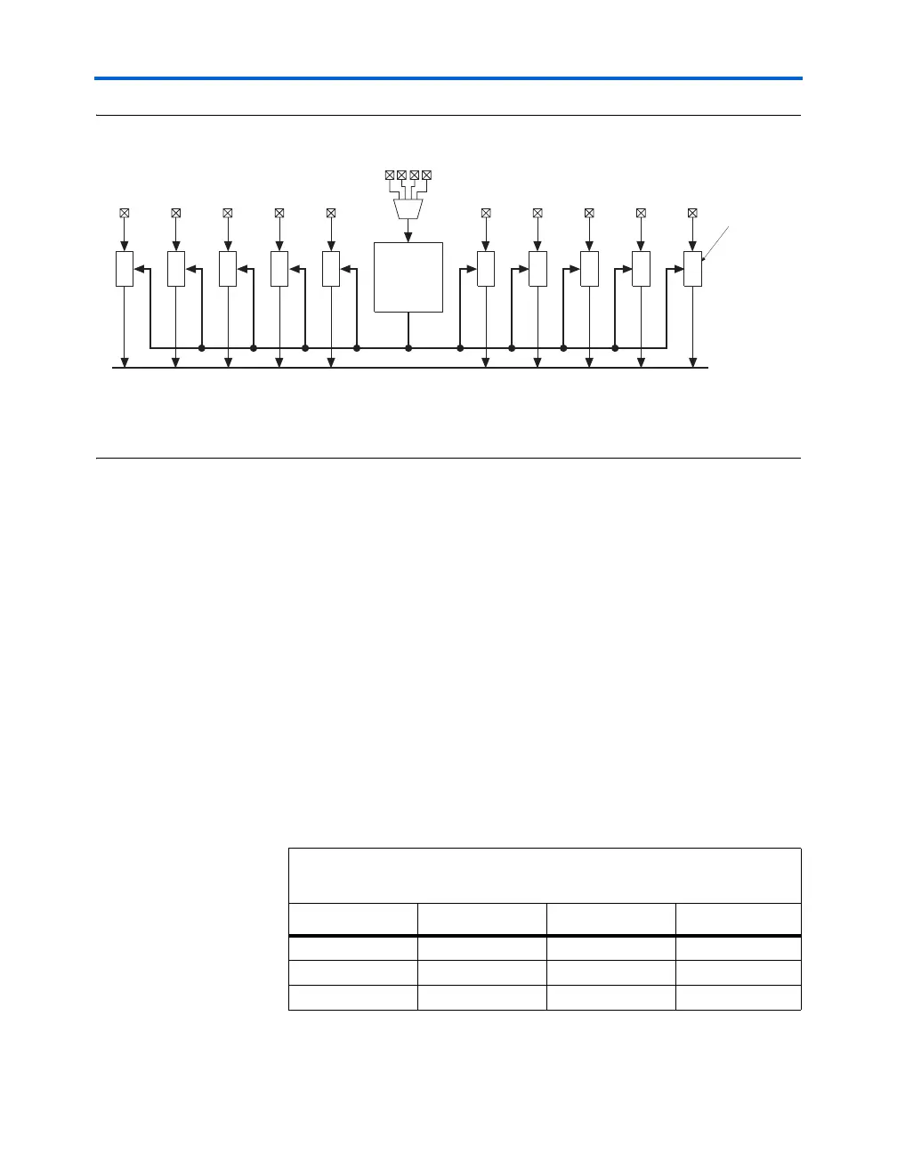
Figure 3–8. DQS & DQSn Pins & the DQS Phase-Shift Circuitry Note (1)
Notes to Figure 3–8:
(1) There are up to 10 DQS and DQSn pins available on the top or the bottom of the Stratix and Stratix GX devices.
(2) Clock pins CLK[15..12]p feed the phase-shift circuitry on the top of the device and clock pins CLK[7..4]p feed
the phase circuitry on the bottom of the device. The reference clock can also be used in the logic array.
The phase-shift circuitry is only used during read transactions where the
DQS pins are acting as input clocks or strobes. The phase-shift circuitry
can shift the incoming DQS signal by 0°, 72°, and 90°. The shifted DQS
signal is then inverted and used as a clock or a strobe at the DQ IOE input
registers.
f Refer to the DC & Switching Characteristics chapter in volume 1 of the
Stratix Device Handbook for frequency limits regarding the 72 and 90°
phase shift for DQS.
The DQS phase-shift circuitry is bypassed when 0° shift is chosen. The
routing delay between the pins and the IOE registers is matched with
high precision for both the DQ and DQS signal when the 72° or 90° phase
shift is used. With the 0° phase shift, the skew between DQ and the DQS
signals at the IOE register has been minimized. See Table 3–4 for the
Quartus II software reported number on the DQ and DQS path to the IOE
when the DQS is set to 0° phase shift.
DQS
Pin
DQS
Pin
DQS
Pin
DQS
Pin
DQS
Pin
DQS
Pin
DQS
Pin
DQS
Pin
DQS
Pin
DQS
Pin
Phase Shift
Reference
Circuit
Δ t Δ t Δ t Δ t Δ t Δ t Δ t Δ t Δ t Δ t
DQS Bus
Compensated
Delay Elemen
CLK[15..12]
(2)
Table 3–4. Quartus II Reported Number on the DQS Path to the
IOE Note (1)
Speed Grade DQ2IOE DQS2IOE Unit
-5 0.908 1.008 ns
-6 0.956 1.061 ns
-7 1.098 1.281 ns