4–36 Altera Corporation
Stratix Device Handbook, Volume 2 June 2006
I/O Pad Placement Guidelines
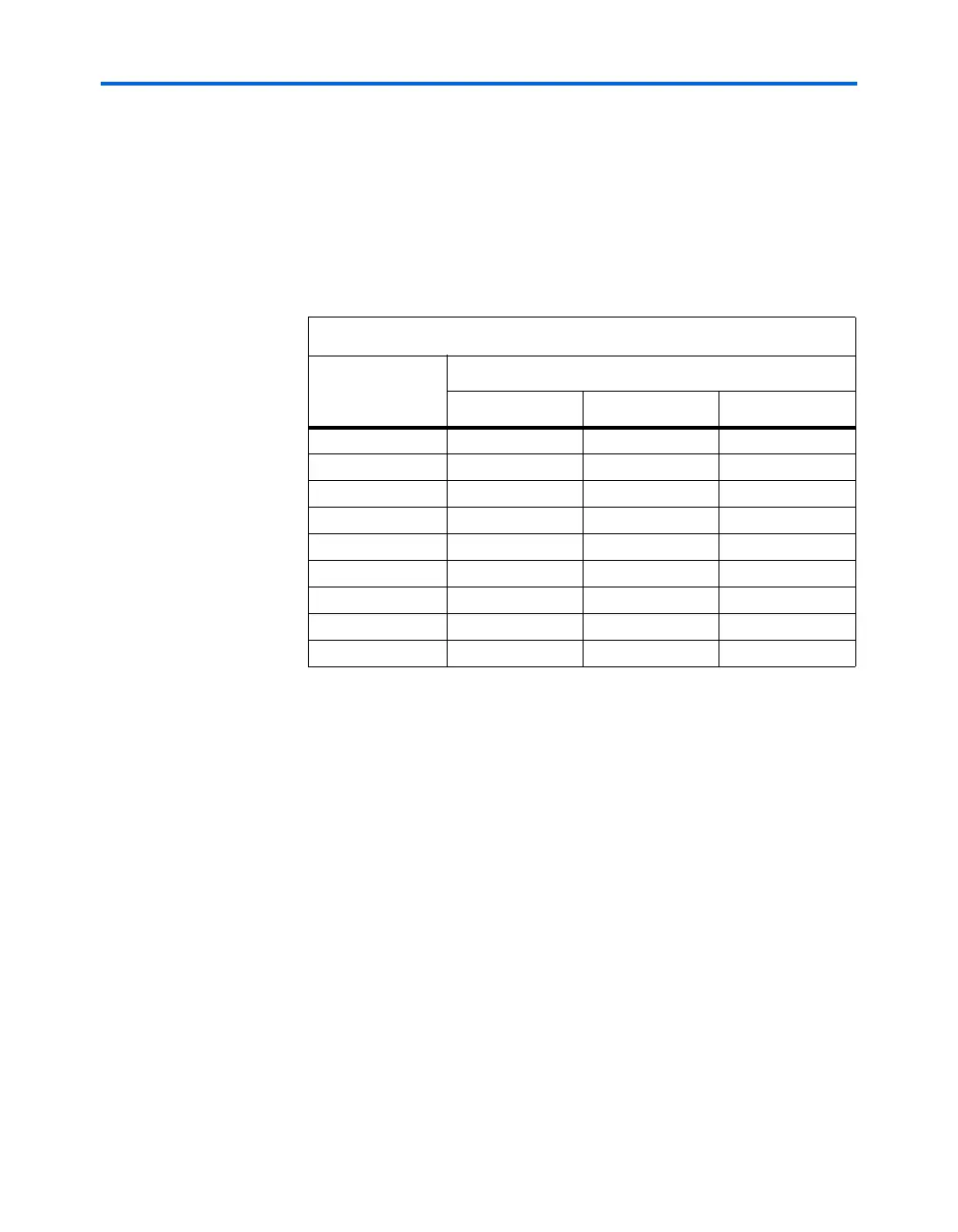
Table 4–12 shows the DC current specification per pin for each I/O
standard. I/O standards not shown in the table do not exceed these
current limitations.
f For more information on Altera device packaging, see the Package
Information for Stratix Devices chapter in the Stratix Device Handbook,
Volume 2.
Table 4–12. I/O Standard DC Specification Note (1)
Pin I/O Standard
I
PIN
(mA)
3.3-V V
CCIO
2.5-V V
CCIO
1.5-V V
CCIO
GTL 40 40 -
GTL+ 34 34 -
SSTL-3 Class I 8 - -
SSTL-3 Class II 16 - -
CTT 8 - -
SSTL-2 Class I - 8.1 -
SSTL-2 Class II - 16.4 -
HSTL Class I - - 8
HSTL Class II - - 16
Note to Table 4–12:
(1) The current rating on a V
REF
pin is less than 10μA.
Σ
pin + 9
pin
I
pin
< 164 mA