5–8 Altera Corporation
Stratix Device Handbook, Volume 2 July 2005
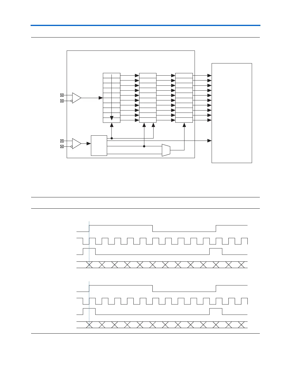
Principles of SERDES Operation
Figure 5–3. Stratix High-Speed Interface Deserialized in ×10 Mode
Notes to Figure 5–3:
(1) W = 1, 2, 4, 7, 8, or 10.
J = 4, 7, 8, or 10.
W does not have to equal J. When J = 1 or 2, the deserializer is bypassed. When J = 2, the device uses DDRIO registers.
(2) This figure does not show additional circuitry for clock or data manipulation.
Figure 5–4. Receiver Timing Diagram
PD0
PD1
PD2
PD3
PD4
PD5
PD6
PD7
PD8
PD9
PD0
PD1
PD2
PD3
PD4
PD5
PD6
PD7
PD8
PD9
PD0
PD1
PD2
PD3
PD4
PD5
PD6
PD7
PD8
PD9
Stratix
Logic Array
Receiver Circuit
Serial Shift
Registers
Parallel
Registers
Parallel
Registers
Fast
PLL (2)
RXIN+
RXIN−
RXCLKIN+
RXCLKIN−
×
W
×
W
/
J (1)
RXLOADEN
TXLOADEN
RXLOADEN
Internal ×1 clock
Internal ×10 clock
Receiver
data input
n – 1 n – 0 9 8 7 6 5 4 3 2 1 0
RXLOADEN
Internal ×1 clock
Internal ×10 clock
Receiver
data input
n – 1 n – 0 9 8 7 6 5 4 3 2 1 0