Altera Corporation 5–71
July 2005 Stratix Device Handbook, Volume 2
High-Speed Differential I/O Interfaces in Stratix Devices
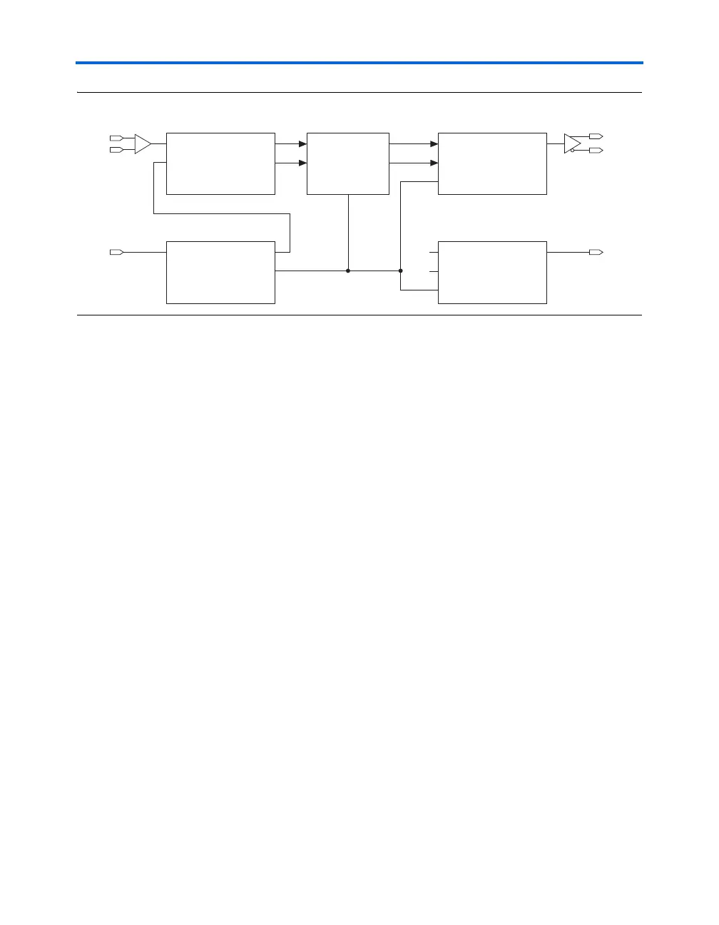
Figure 5–44. LVDS x2 Mode Schematic Using DDR I/O Circuitry
The transmitter output clock requires extra DDR output circuitry that has
the input high and input low connected to V
CC
and GND respectively. The
output clock frequency is the same as the input frequency of the DDR
output circuitry.
Other Modes
For other modes, you can still to use the DDR circuitry for better
frequency performance. You can use either the LEs or the M512 RAM
block for the deserialization.
M512 RAM Block as Serializer/Deserializer Interface
In addition to using the DDR circuitry and the M512 RAM block, you
need two extra counters per memory block to provide the address for the
memory: a fast counter powering up at 0 and a slow counter powering up
at 2. The M512 RAM block is configured as a simple dual-port memory
block, where the read enable and the write enable signals are always tied
high. Figures 5–45 and 5–46 show the block diagram for the SERDES
bypass receiver and SERDES bypass transmitter, respectively.
datain[0]
inclock
dataout_h[0]
dataout_l[0]
DDIO In
datain_h[0]
datain_l[0]
outclock
dataout[0]
DDIO Out
datain_h[0]
datain_l[0]
outclock
dataout[0]
DDIO Out
inclock /1 clock1
/2 clock0
RX_PLL
Custom Logic
V
CC
GND
RXp
RXn
rx_inclk
TXp
TXn
tx_outclk