8–14 Altera Corporation
Stratix Device Handbook, Volume 2 July 2005
Interfaces
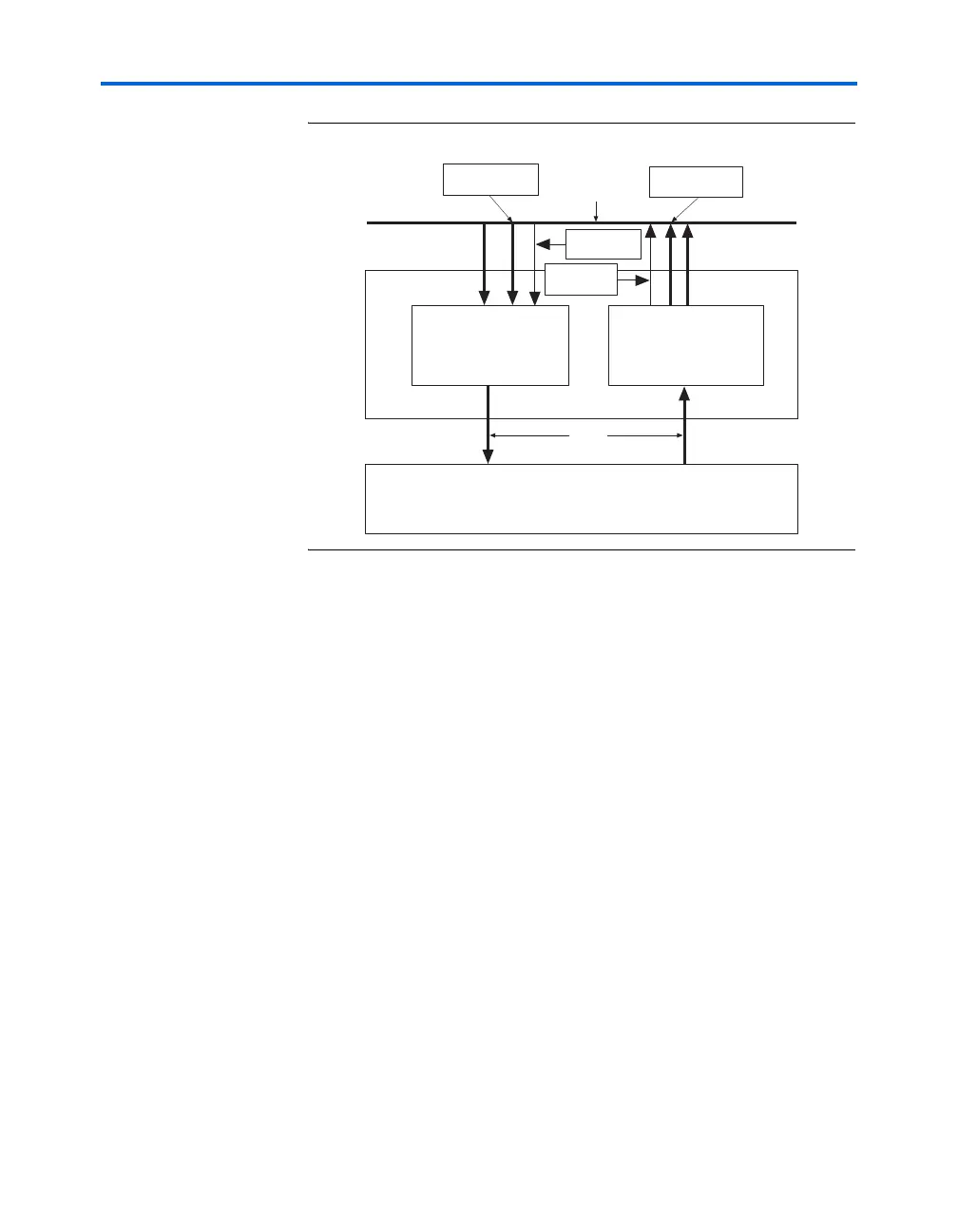
Figure 8–10. XGMII Functional Block Diagram
The 32 TXD and four TXC signals as well as the 32 RXD and four RXC
signals are organized into four data lanes. The four lanes in each direction
share a common clock (TX_CLK for transmit and RX_CLK for receive). The
four lanes are used in round-robin sequence to carry an octet stream
(8 bits of data per lane). The reconciliation sublayer generates continuous
data or control characters on the transmit path and expects continuous
data or control characters on the receive path.
Implementation
XGMII uses the 1.5-V HSTL I/O standard. Stratix and Stratix GX devices
support the 1.5-V HSTL Class I and Class II I/O standard (EIA/JESD8-6).
The standard requires a differential input with an external reference
voltage (V
REF
) of 0.75 V, as well as a termination voltage V
TT
of 0.75 V, to
which termination resistors are connected. The HSTL Class I standard
requires a 1.5-V V
CCIO
voltage, which is supported by Stratix and
Stratix GX devices.
Figure 8–11 shows the 32-bit full-duplex 1.5-V HSTL implementation of
XGMII.
PCS
Transmit
PCS
PCS
Receive
PMA
XGMII
tx_data[15..0] rx_data[15..0]
TXD[31..0] RXD[31..0]
XSBI
TX_CLK
RX_CLK
RXC[3..0]
TXC[3..0]