Altera Corporation 8–15
July 2005 Stratix Device Handbook, Volume 2
Implementing 10-Gigabit Ethernet Using Stratix & Stratix GX Devices
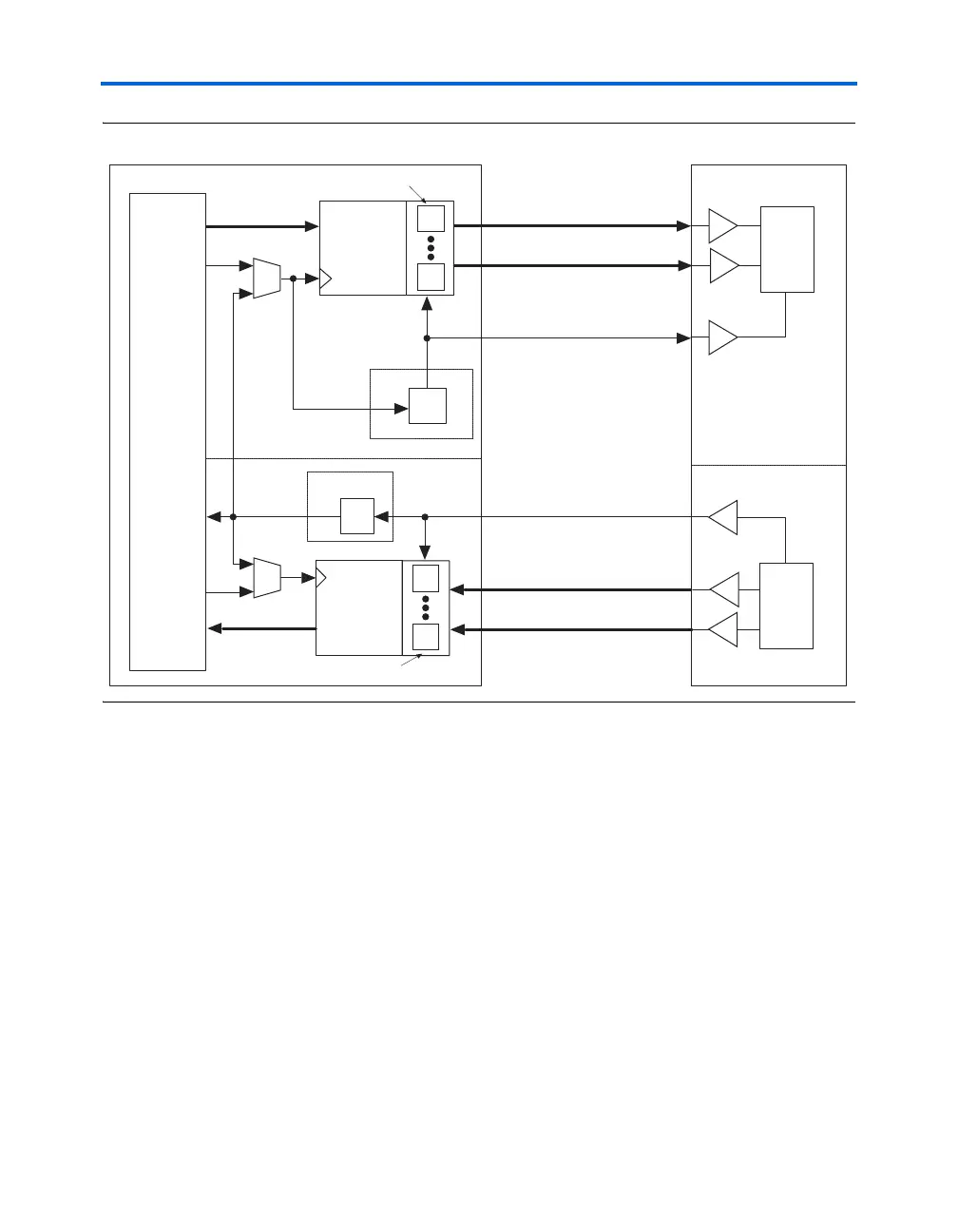
Figure 8–11. Stratix & Stratix GX XGMII Implementation
For this implementation, the shift register clocks can either be generated
from a divided down MAC reconciliation sublayer transmitter clock
(MAC_TXCLK), or the asynchronous core clock, or both if using a FIFO
buffer.
Figure 8–12 shows one channel of the output half of XGMII. Data that is
transmitted from the PCS to the MAC reconciliation sublayer starts at the
core of the Stratix or Stratix GX device and travels to the shift register. The
shift register takes in the parallel data (even bits sent to the top register
and odd bits sent to the bottom register) and serializes the data. After the
data is serialized, it travels to the double data rate (DDR) output circuitry,
which is clocked with the ×4 clock from the PLL. Out of the DDR output
circuitry, the data drives off-chip along with the ×4 clock. This transaction
creates the DDR relationship between the clock and the data output. This
implementation only shows one channel, but can be duplicated to include
all 32 bits of the RX_D signal and all 4 bits of the RX_C signal.
Shift
Register
Shift
Register
×4
÷4
Clk
Data
Clk
Data
Transmitter
Receiver
MAC (RS)
RX_D[31..0]
MAC_RXCLK
MAC_TXCLK
TX_D[31..0]
Receiver
Transmitter
Stratix & Stratix GX PCS
RX_C[3..0]
TX_C[3..0]
DDR Input Circuitry
DDR Output Circuitry
PLL1
PLL2
Stratix &
Stratix GX
Logic Array