8–16 Altera Corporation
Stratix Device Handbook, Volume 2 July 2005
Interfaces
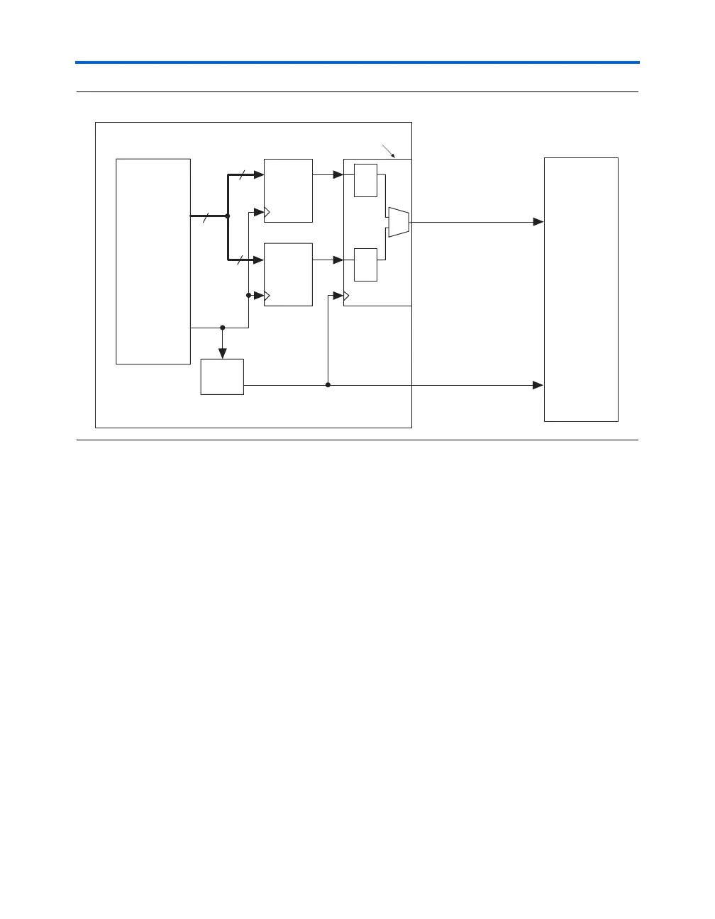
Figure 8–12. Stratix & Stratix GX XGMII Output Implementation (One Channel)
Figure 8–13 shows one channel of the input half of the XGMII interface.
From the receiver side, the DDR data is captured from the MAC to the
Stratix and Stratix GX PCS DDR input circuitry. The serial data is
separated into two individual data streams with the even bits routed to
the top register and odd bits routed to the bottom register. The DDR input
circuitry produces two output data streams that go into the shift registers.
From the shift registers, the data is deserialized using the clock from the
MAC, combining into an 8-bit word. This parallel data goes to a register
that is clocked by the divide-by-4 clock from the PLL. This data and clock
go to the Stratix and Stratix GX core. This implementation shows only one
channel, but can be duplicated to include all 32 bits of the TX_D signal and
all 4 bits of the TX_C signal.
RX_D[0]
8
4
MAC
Receiver
MAC_RXCLK
Stratix & Stratix GX PCS Output
156.25 MHz
312.5 Mbps
4
Shift
Register
D0,D2,D4,D6
D1,D3,D5,D7
DFF
DFF
PLL
×4
DATA
CLK
DATA
CLK
39.0625 MHz
156.25 MHz
DDR Output Circuitry
Shift
Register
Stratix &
Stratix GX
Logic Array