Altera Corporation 11–31
July 2005 Stratix Device Handbook, Volume 2
Configuring Stratix & Stratix GX Devices
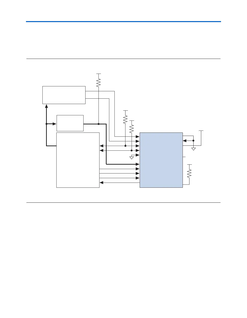
Figure 11–16 shows the PPA configuration circuit. An optional address
decoder controls the device’s nCS and CS pins. This decoder allows the
microprocessor to select the Stratix or Stratix GX device by accessing a
particular address, simplifying the configuration process.
Figure 11–16. PPA Configuration Circuit
Note to Figure 11–16:
(1) The pull-up resistor should be connected to the same supply voltage as the Stratix or Stratix GX device.
The device’s nCS or CS pins can be toggled during PPA configuration if
the design meets the specifications for t
CSSU
, t
WSP
, and t
CSH
given in
Table 11–10 on page 11–36. The microprocessor can also directly control
the nCS and CS signals. You can tie one of the nCS or CS signals to its
active state (i.e., nCS may be tied low) and toggle the other signal to
control configuration.
Stratix and Stratix GX devices can serialize data internally without the
microprocessor. When the Stratix or Stratix GX device is ready for the
next byte of configuration data, it drives RDYnBSY high. If the
microprocessor senses a high signal when it polls RDYnBSY, the
microprocessor strobes the next byte of configuration data into the
device. Alternatively, the nRS signal can be strobed, causing the
RDYnBSY signal to appear on DATA7. Because RDYnBSY does not need to
MSEL2
MSEL1
MSEL0
Stratix Device
DCLK
10 kΩ
10 kΩ
10 kΩ
10 kΩ
nCS
CS
CONF_DONE
nSTATUS
nCE
DATA[7..0]
nWS
nRS
nCONFIG
RDYnBSY
Address Decoder
V
CC
V
CC
V
CC
ADDR
Microprocessor
V
CC
V
CC
Memory
ADDR
DATA[7..0]
GND
nCEO
N.C.
(1)
(1)
(1)
(1)
GND