11–38 Altera Corporation
Stratix Device Handbook, Volume 2 July 2005
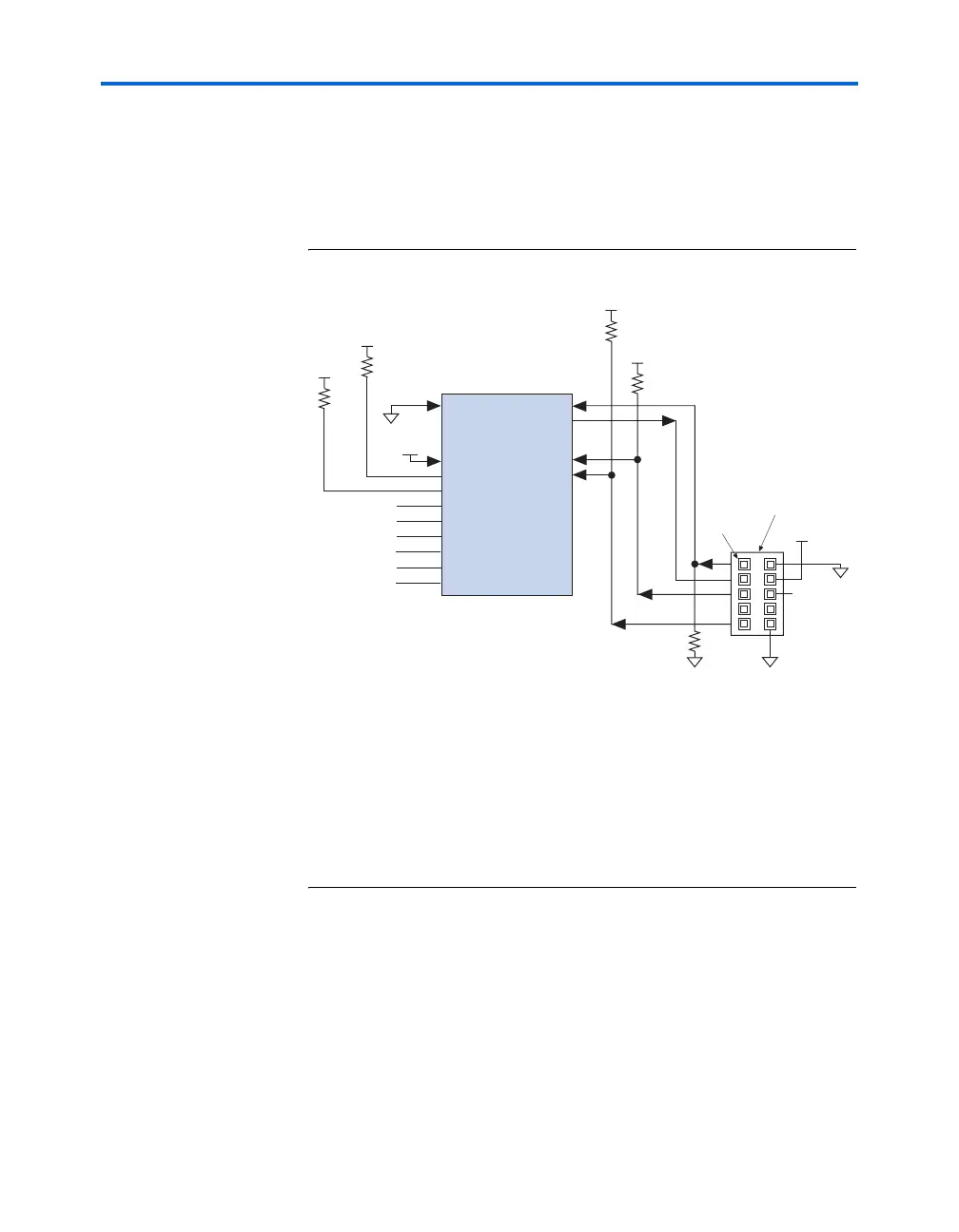
Configuration Schemes
During JTAG configuration, data is downloaded to the device on the PCB
through the MasterBlaster or ByteBlasterMV header. Configuring devices
through a cable is similar to programming devices in-system. One
difference is to connect the TRST pin to V
CC
to ensure that the TAP
controller is not reset. See Figure 11–20.
Figure 11–20. JTAG Configuration of a Single Device
Notes to Figure 11–20:
(1) You should connect the pull-up resistor to the same supply voltage as the
download cable.
(2) You should connect the nCONFIG, MSEL0, and MSEL1 pins to support a non-JTAG
configuration scheme. If you only use JTAG configuration, connect nCONFIG to
V
CC
, and MSEL0, MSEL1, and MSEL2 to ground. Pull DATA0 and DCLK to high or
low.
(3) V
IO
is a reference voltage for the MasterBlaster output driver. V
IO
should match the
device’s V
CCIO
. See the MasterBlaster Serial/USB Communications Cable Data Sheet for
this value.
To configure a single device in a JTAG chain, the programming software
places all other devices in BYPASS mode. In BYPASS mode, devices pass
programming data from the TDI pin to the TDO pin through a single
bypass register without being affected internally. This scheme enables the
programming software to program or verify the target device.
Configuration data driven into the device appears on the TDO pin one
clock cycle later.
nCE
MSEL0
MSEL1
nCONFIG
CONF_DONE
V
CC
(1)
V
CC
(1)
GND
V
CC
V
CC
GND
V
CC
(2)
(2)
(2)
V
CC
(1)
1 kΩ
10 kΩ
10 kΩ
1 kΩ
nSTATUS
Pin 1
MasterBlaster or ByteBlasterMV
10-Pin Male Header
(Top View)
GND
TRST
TCK
TDO
TMS
TDI
1 kΩ
GND
VIO (3)
Stratix or
Stratix GX Device
MSEL2
DATA0
DCLK
(2)
(2)
(2)