Altera Corporation 11–43
July 2005 Stratix Device Handbook, Volume 2
Configuring Stratix & Stratix GX Devices
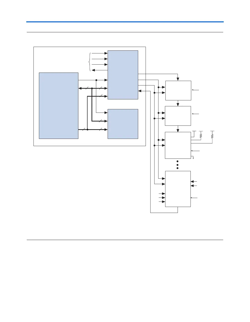
Figure 11–23. Embedded System Block Diagram
Notes to Figure 11–23:
(1) Connect the nCONFIG, MSEL2, MSEL1, and MSEL0 pins to support a non-JTAG configuration scheme. If your design
only uses JTAG configuration, connect the nCONFIG pin to V
CC
and the MSEL2, MSEL1, and MSEL0 pins to ground.
(2) Pull DATA0 and DCLK to either high or low.
Both JTAG connection methods should include space for the
MasterBlaster or ByteBlasterMV header connection. The header is useful
during prototyping because it allows you to verify or modify the Stratix
or Stratix GX device’s contents. During production, you can remove the
header to save cost.
TDI
TMS
TCK
TDO
TDI
TMS
TCK
TDO
TDI
TMS
TCK
TDO
TDI
TMS
TCK
TDO
TDI
TMS
TCK
TDO
ControlControl
d[3..0]d[7..0]
adr[19..0]
Control
d[7..0]
adr[19..0]adr[19..0]
Interface
Logic
(Optional)
Any JTAG
Device
EPROM or
System
Memory
to/from ByteBlasterMV
Embedded
Processor
Embedded System
8
8
4
20
2020
MAX
®
9000,
MAX 9000A,
MAX 7000S,
MAX 7000A,
MAX 7000AE,
or MAX 3000
Device
Cyclone FPGA
TDI
TMS
TRST
CONF_DONE
nSTATUS
nCONFIG
MSEL0
MSEL1
nCE
TCK
TDO
Any Cyclone,
FLEX 10K,
FLEX 10KA,
FLEX10KE,
APEX 20K,
or APEX 20KE
Device
10 kΩ10 kΩ
V
CC
V
CC
V
CC
GND
DATA0
DCLK
nCONFIG
(2)
(2)
(1)
(1)
(1)
MSEL1
MSEL0