Altera Corporation 11–55
July 2005 Stratix Device Handbook, Volume 2
Configuring Stratix & Stratix GX Devices
nCEO
N/A All Multi-
Device
Schemes
Output Output that drives low when device
configuration is complete. In single device
configuration, this pin is left floating. In multi-
device configuration, this pin feeds the next
device’s
nCE pin. The nCEO of the last device
in the chain is left floating.
The voltage levels driven out by this pin are
dependent on the V
CCIO
of the I/O bank it
resides in.
DCLK
N/A Synchronous
configuration
schemes
(PS, FPP)
Input
(PS, FPP)
In PS and FPP configuration,
DCLK is the clock
input used to clock data from an external
source into the target device. Data is latched
into the FPGA on the rising edge of
DCLK.
In PPA mode,
DCLK should be tied high to V
CC
to prevent this pin from floating.
After configuration, this pin is tri-stated. In
schemes that use a configuration device,
DCLK is driven low after configuration is done.
In schemes that use a control host,
DCLK
should be driven either high or low, whichever
is more convenient. Toggling this pin after
configuration does not affect the configured
device. This pin uses Schmitt trigger input
buffers.
DATA0
I/O PS, FPP, PPA Input Data input. In serial configuration modes, bit-
wide configuration data is presented to the
target device on the
DATA0 pin. The V
IH
and
V
IL
levels for this pin are dependent on the
V
CCIO
of the I/O bank that it resides in.
After configuration,
DATA0 is available as a
user I/O and the state of this pin depends on
the Dual-Purpose Pin settings.
After configuration, EPC1 and EPC1441
devices tri-state this pin, while enhanced
configuration and EPC2 devices drive this pin
high.
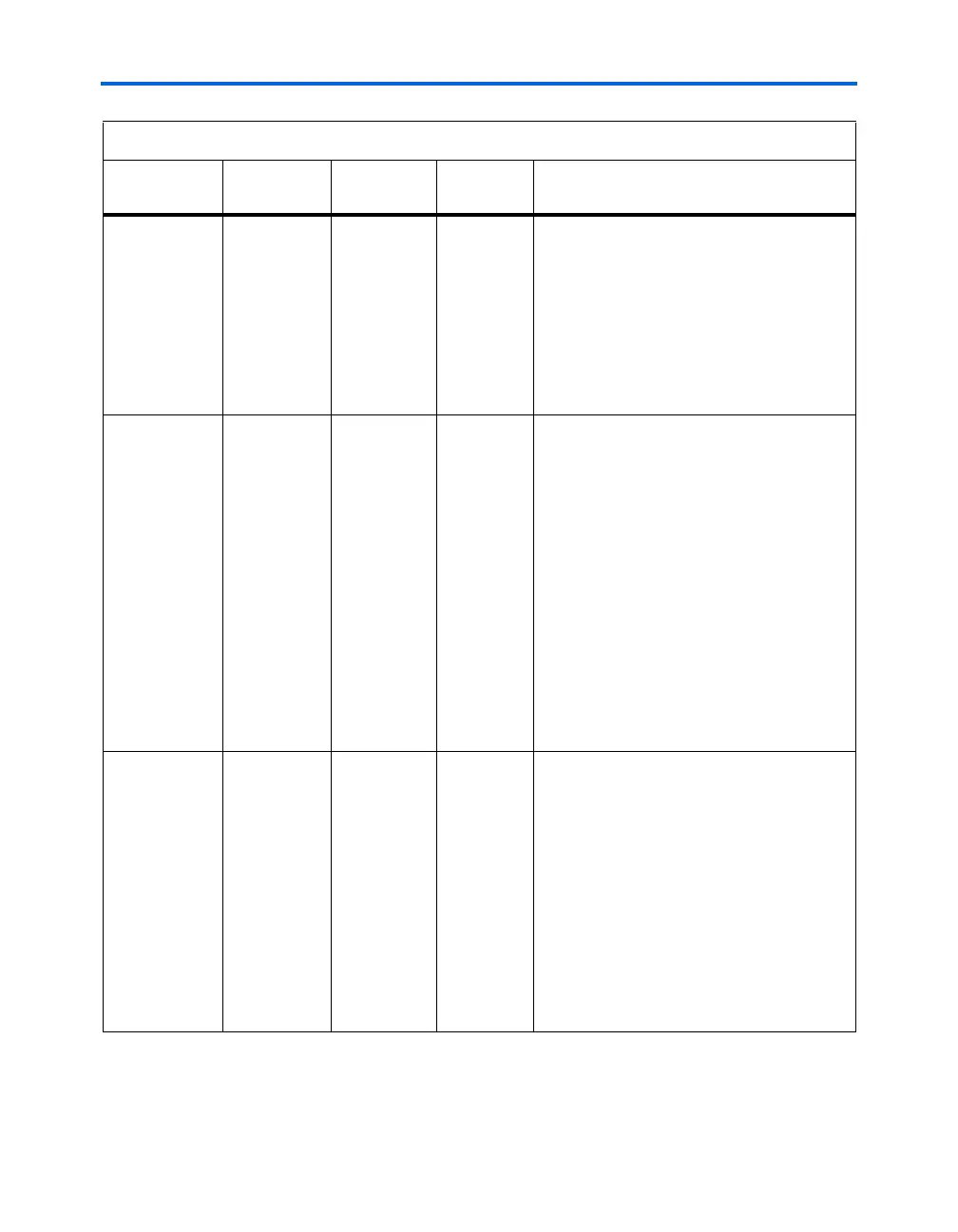
Table 11–15. Dedicated Configuration Pins on the Stratix or Stratix GX Device (Part 5 of 8)
Pin Name User Mode
Configuration
Scheme
Pin Type Description