2–2 Altera Corporation
Stratix Device Handbook, Volume 2 July 2005
TriMatrix Memory
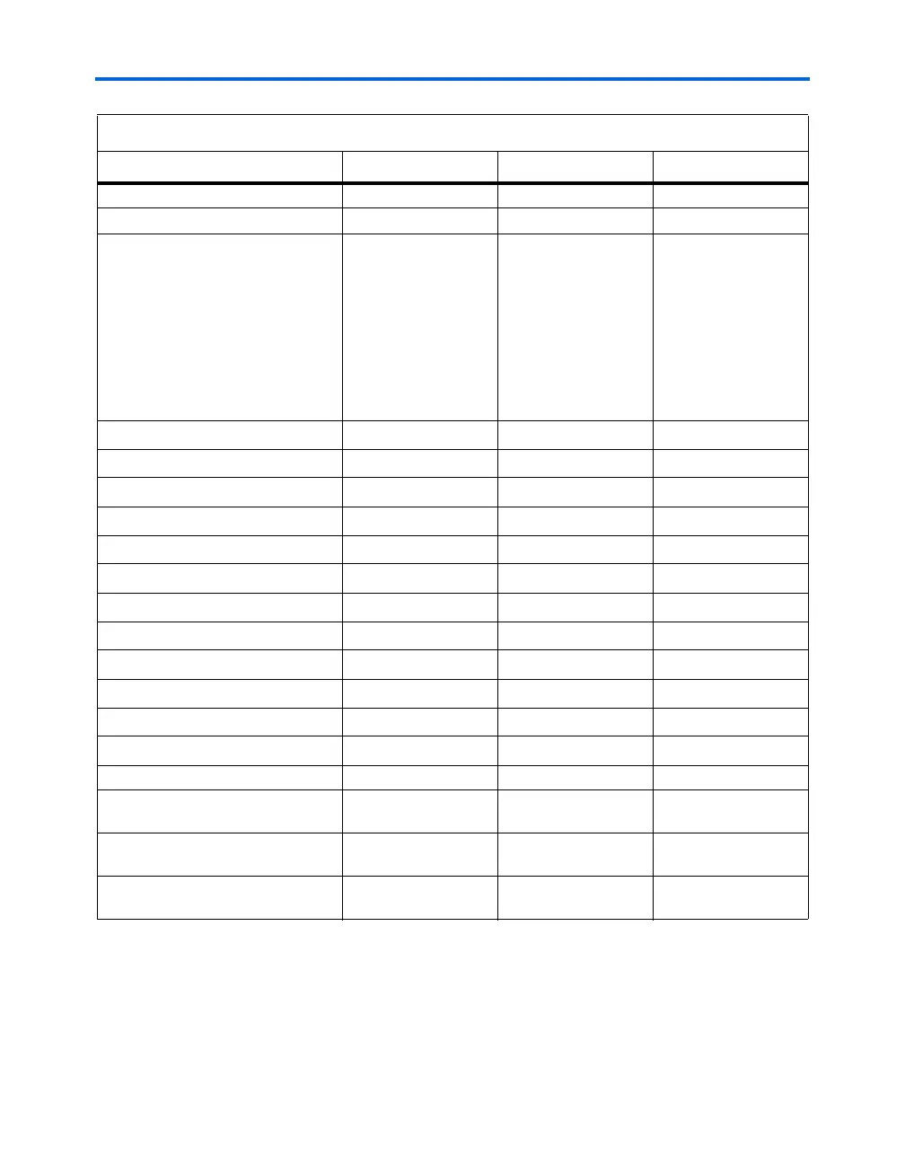
Table 2–1. Summary of TriMatrix Memory Features
Feature M512 Block M4K Block M-RAM Block
Performance 319 MHz 290 MHz 287 MHz
Total RAM bits (including parity bits) 576 4,608 589,824
Configurations 512 × 1
256 × 2
128 × 4
64 × 8
64 × 9
32 × 16
32 × 18
4K × 1
2K × 2
1K × 4
512 × 8
512 × 9
256 × 16
256 × 18
128 × 32
128 × 36
64K × 8
64K × 9
32K × 16
32K × 18
16K × 32
16K × 36
8K × 64
8K × 72
4K × 128
4K × 144
Parity bits
vvv
Byte enable
vv
Single-port memory
vvv
Simple dual-port memory
vvv
True dual-port memory
vv
Embedded shift register
vv
ROM
vv
FIFO buffer
vvv
Simple dual-port mixed width support
vvv
True dual-port mixed width support
vv
Memory initialization file (.mif)
vv
Mixed-clock mode
vvv
Power-up condition Outputs cleared Outputs cleared Outputs unknown
Register clears Input and output
registers (1)
Input and output
registers (2)
Output registers
Same-port read-during-write New data available at
positive clock edge
New data available at
positive clock edge
New data available at
positive clock edge
Mixed-port read-during-write Outputs set to
unknown or old data
Outputs set to
unknown or old data
Unknown output
Notes to Ta b le 2 – 1 :
(1) The rden register on the M512 memory block does not have a clear port.
(2) On the M4K block, asserting the clear port of the rden and byte enable registers drives the output of these registers
high.