2–22 Altera Corporation
Stratix Device Handbook, Volume 2 July 2005
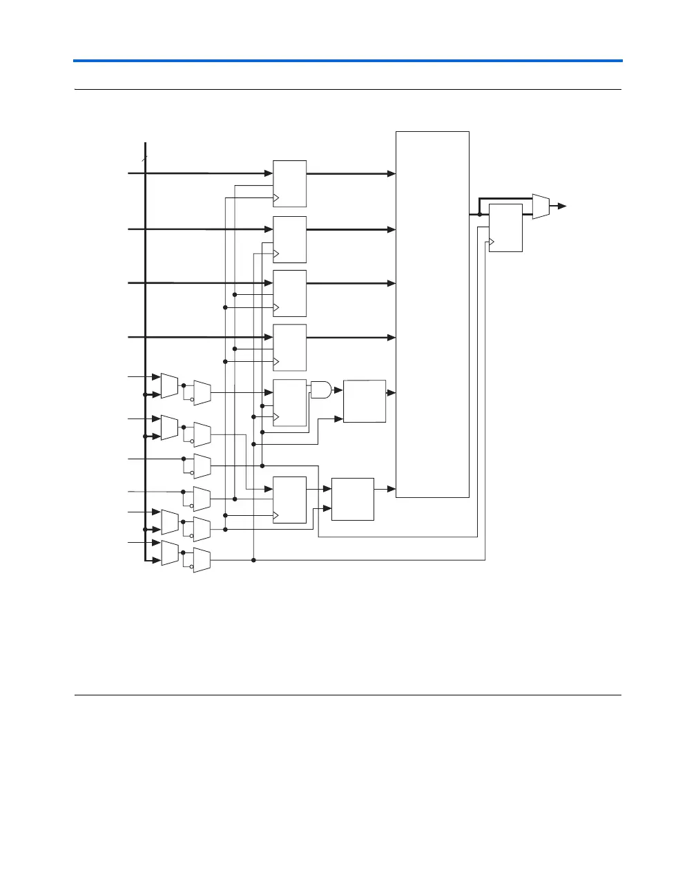
Clock Modes
Figure 2–12. Read/Write Clock Mode in Simple Dual-Port Mode Notes (1), (2), (3)
Notes to Figure 2–12:
(1) For more information on the MultiTrack interconnect, see the Stratix Device Family Data Sheet section of the Stratix
Device Handbook, Volume 1 or the Stratix GX Device Family Data Sheet section of the Stratix GX Device Handbook,
Volume 1.
(2) All registers shown have asynchronous clear ports, except when using the M-RAM. M-RAM blocks have
asynchronous clear ports on their output registers only.
(3) Violating the setup or hold time on the address registers could corrupt the memory contents. This applies to both
read and write operations.
8
D
ENA
Q
D
ENA
Q
D
ENA
Q
D
ENA
Q
D
ENA
Q
data[ ]
D
ENA
Q
wraddress[ ]
address[ ]
Memory Block
256 × 16
512 × 8
1,024 × 4
2,048 × 2
4,096 × 1
Data In
Read Address
Write Address
Write Enable
Read Enable
Data Out
rdclocken
wrclocken
wrclock
rdclock
wren
rden
8 LAB Row
Clocks
To MultiTrac
Interconnect
D
ENA
Q
byteena[ ]
Byte Enable
Write
Pulse
Generator
Read
Pulse
Generator