126 www.xilinx.com Virtex-6 FPGA GTX Transceivers User Guide
UG366 (v2.5) January 17, 2011
Chapter 2: Shared Transceiver Features
Ports and Attributes
Table 2-18 defines the DRP ports.
There are no DRP attributes.
Note:
Attributes that have an impact on the entire Quad (the cluster of four GTX transceivers) are
set by writing to the DRP of the first transceiver in the Quad. The first transceiver in the Quad has the
lowest Y coordinates. Refer to Implementation, page 41 for details on transceiver placement and
numbering.
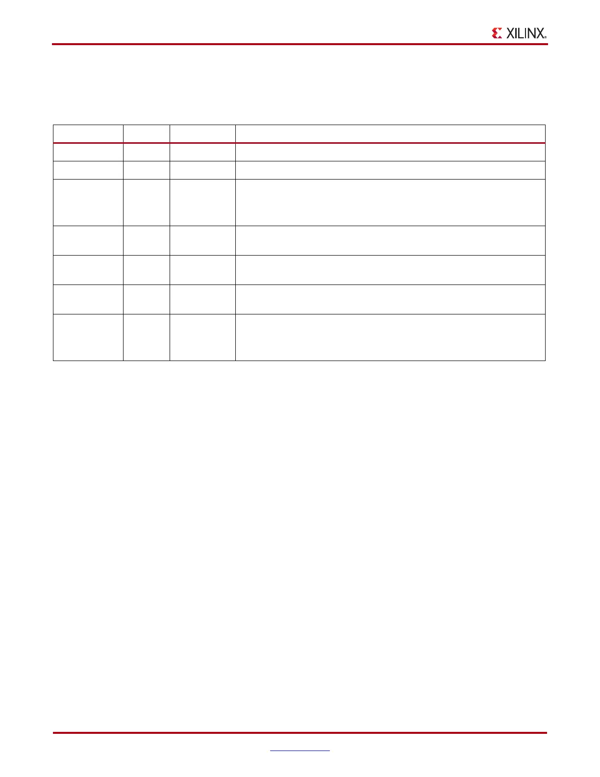
Table 2-18: DRP Ports
Port Dir Clock Domain Description
DADDR[7:0] In DCLK DRP address bus.
DCLK In N/A DRP interface clock.
DEN In DCLK DRP enable signal.
0: No read or write operation performed.
1: Enables a read or write operation.
DI[15:0] In DCLK Data bus for writing configuration data from the FPGA logic resources to
the GTX transceiver.
DRDY Out DCLK Indicates operation is complete for write operations and data is valid for
read operations.
DRPDO[15:0] Out DCLK Data bus for reading configuration data from the GTX transceiver to the
FPGA logic resources.
DWE In DCLK DRP write enable.
0: Read operation when DEN is 1.
1: Write operation when DEN is 1.

 Loading...

