276 www.xilinx.com Virtex-6 FPGA GTX Transceivers User Guide
UG366 (v2.5) January 17, 2011
Chapter 5: Board Design Guidelines
Managing Unused GTX Transceivers
In many applications, only a portion of the GTX transceivers are required. There are
considerations for managing the unused GTX transceivers that affect such things as power
consumption of the Virtex-6 FPGA. When considering which Quads to use in an
application, the organization of the package power planes needs to be taken into account.
Power can be utilized efficiently when there are multiple analog power planes in the
package. If only a small number of the Quads are to be used, it might be possible to leave
some of them completely unpowered.
The criteria for powering a GTX QUAD is based on whether the GTX transceivers will be
permanently unused or whether they will be used at a later date. If a GTX transceiver is
ever intended to be used, it must be powered whenever the FPGA is powered up. If the
GTX transceiver will never be used, the transceiver bank can be unpowered. Connections
to unused GTX transceivers (including power supplies) are covered in the following
sections.
Analog Power Supply Pins
The Quad analog power supply pins, MGTAVCC and MGTAVTT, have planes inside the
package. Some packages have two planes for each of these analog power supplies,
designated as north and south. Therefore, the Quads in a column are grouped by their
common analog power supply connections into banks. There are north and south banks of
Quads. For each of the analog power supplies, pins for all of the north Quads are
connected to the same plane inside the package. Similarly, for each of the analog power
supplies, the pins for the south bank of Quads are connected to the same plane inside the
package. As a result, there are four Quad analog power supply planes inside the package.
Inside the package are two MGTAVCC power planes and two MGTAVTT power planes.
Refer to Table 5-2 for a description of the connected Quads.
In Table 5-2, there are two types of groupings of the Quads in a column.
• Devices with two banks of Quads in a column:
• North bank of Quads
• South bank of Quads
• Devices with one bank of Quads in a column
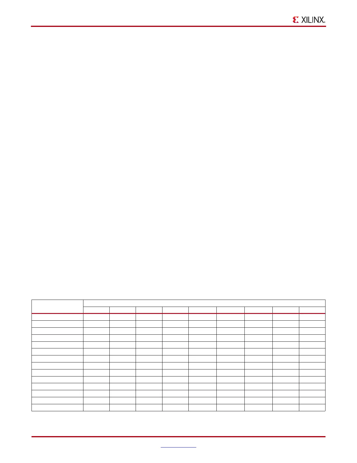
Table 5-2: Connected Quads
Device
Quad
(1)
MGT110 MGT111 MGT112 MGT113 MGT114 MGT115 MGT116 MGT117 MGT118
XC6VLX75T-FF484
(2)
Common
(3)
Common
XC6VLX75T-FF784
(2)
Common Common Common
XC6VLX130T-FF484
(2)
Common Common
XC6VLX130T-FF784
(2)
Common Common Common
XC6VLX130T-FF1156 South
(4,6)
South South North
(5,6)
North
XC6VLX195T-FF784
(2)
Common Common Common
XC6VLX195T-FF1156 South South South North North
XC6VLX240T-FF784
(2)
Common Common Common
XC6VLX240T-FF1156 South South South North North
XC6VLX240T-FF1759 South South South North North North
XC6VLX365T-FF1156 South South South North North
XC6VLX365T-FF1759 South South South North North North
XC6VLX550T-FF1759 South South South South South North North North North
XC6VSX315T-FF1759 South South South North North North

 Loading...

