Virtex-6 FPGA GTX Transceivers User Guide www.xilinx.com 273
UG366 (v2.5) January 17, 2011
Chapter 5
Board Design Guidelines
Overview
This chapter discusses topics related to implementing a design that uses the Virtex®-6
FPGA
GTX transceiver on a printed circuit board (PCB). The GTX transceivers are analog circuits
that require special consideration and attention when designing and implementing them
on a PCB. For a design to perform optimally, the designer requires an understanding of the
functionality of the device pins and needs to attend to issues such as device interfacing,
transmission line impedance and routing, power supply design filtering and distribution,
component selection, and PCB layout and stackup design.
Pin Description and Design Guidelines
GTX Transceiver Pin Descriptions
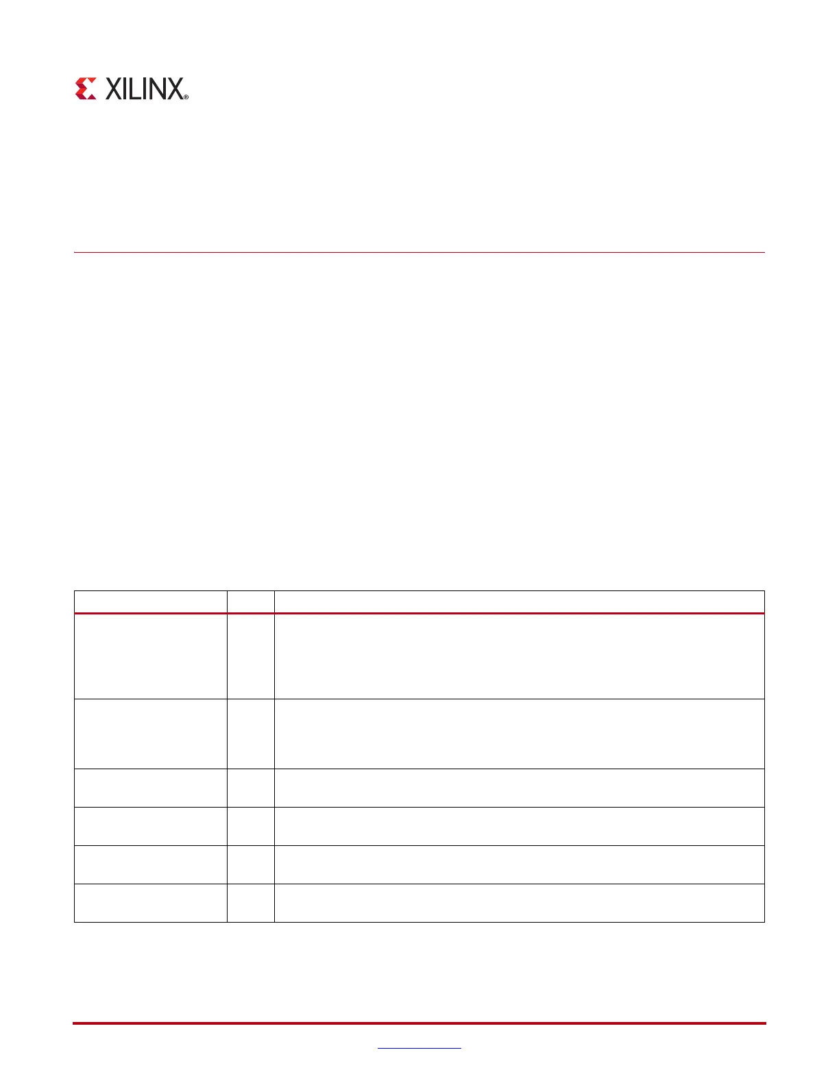
Table 5-1 defines the pins in a Quad.
Table 5-1: Quad Pin Descriptions
Pin Dir Description
MGTAVCC_N
MGTAVCC_S
In
(Pad)
MGTAVCC is the analog supply for the internal analog circuits of the Quad. This
includes the analog circuits for the PLLs, transmitters, and receivers. Most packages
have a north and south bank in the package for MGTAVCC. Refer to the package pin
definitions to identify the power supply bank that is associated with the specific
Quad. The nominal voltage is 1.0 V
DC
.
MGTAVTT_N
MGTAVTT_S
In
(Pad)
MGTAVTT is the analog supply for the transmitter and receiver termination circuits
of the Quad. Most packages have a north and south bank in the package for
MGTAVTT. Refer to the package pin definitions to identify the power supply bank
that is associated with the specific Quad. The nominal voltage is 1.2 V
DC
.
MGTAVTTRCAL In
(Pad)
Bias current supply for the termination resistor calibration circuit. See Termination
Resistor Calibration Circuit, page 274 for more information.
MGTREFCLK0P
MGTREFCLK0N
In
(Pad)
Differential clock input pin pair for the reference clock of the Quad.
MGTREFCLK1P
MGTREFCLK1N
In
(Pad)
Differential clock input pin pair for the reference clock of the Quad.
MGTRREF In
(Pad)
Calibration resistor input pin for the termination resistor calibration circuit. See
Termination Resistor Calibration Circuit, page 274 for more information.

 Loading...

