Virtex-6 FPGA GTX Transceivers User Guide www.xilinx.com 289
UG366 (v2.5) January 17, 2011
Power Supply and Filtering
Signal BGA Breakout
The receiver, transmitter, and reference clock signals must be routed from the BGA pin
field to destinations on the PCB. The signal routing layers provide the routing resources for
this signal breakout. As shown in Figure 5-14, the signals on the outer rows of BGA pins
can be routed using a microstrip on the top layer. These signals are routed to vias where the
signal is transitioned from the top microstrip layer to striplines on Layer 3. An advantage
to routing the signals from Layer 1 to Layer 3 is that the traces on both layers use the plane
on Layer 2 as the return current reference plane.
X-Ref Target - Figure 5-13
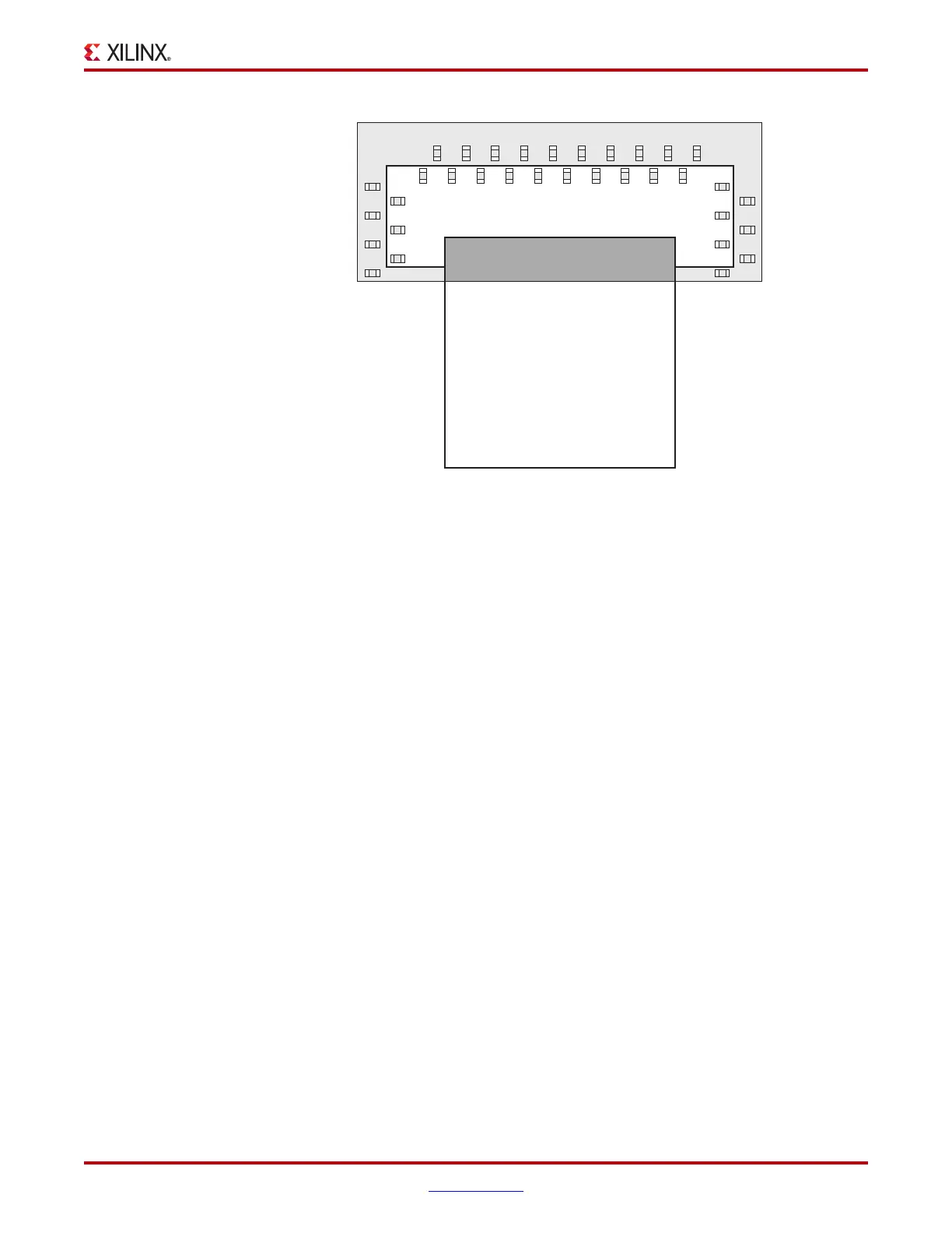
Figure 5-13: Orientation between GTX Transceiver Power Islands and the
Virtex-6 FPGA
Virtex-6
FPGA
MGTAVTT 1.2V Island (Top)
MGTAVCC 1.0V Island (Bottom)
UG366_c5_13_051509
GTX Transceiver Region

 Loading...

