Virtex-6 FPGA GTX Transceivers User Guide www.xilinx.com 113
UG366 (v2.5) January 17, 2011
PLL
For multi-rate designs that require the reference clock source to be changed on the fly, the
TXPLLREFSELDY and RXPLLREFSELDY ports are used to dynamically select the
reference clock source. When the selection has been made, the user design is responsible
for resetting the TX PLL and RX PLL via the active-high GTXTXRESET and GTXRXRESET
ports. Because GTXTXRESET and GTXRXRESET ports are asynchronous, the user design
can simply provide a pulse as short as one clock cycle of the reference clock supported by
the FPGA logic. Refer to the PLL section to confirm if the PLL divider settings are optimal
for both reference clocks.
When bypassing the TX buffer, all of these requirements must be met:
• If the TX PLL supplies the clock for the TX datapath (TX_CLK_SOURCE = “TXPLL”),
the transmitter reference clock must always be toggling.
• If the RX PLL supplies the clock for the TX datapath (TX_CLK_SOURCE = “RXPLL”),
the receiver reference clock must always be toggling.
Refer to TX Buffer Bypass, page 155 for more information.
When bypassing the RX buffer, the receiver reference clock must always be toggling. Refer
to RX Buffer Bypass, page 231 for more information.
PLL
Functional Description
Each GTX transceiver contains one TX PLL and one RX PLL, which allows the TX and RX
datapaths to operate in asynchronous frequencies using different reference clock inputs.
For applications where the TX and RX datapaths operate in the same line rate range, the RX
PLL can be shared between the TX and RX datapaths and the TX PLL can be powered
down to conserve power. The TX or RX PLL in one GTX transceiver cannot be shared with
other GTX transceivers, only within the same transceiver.
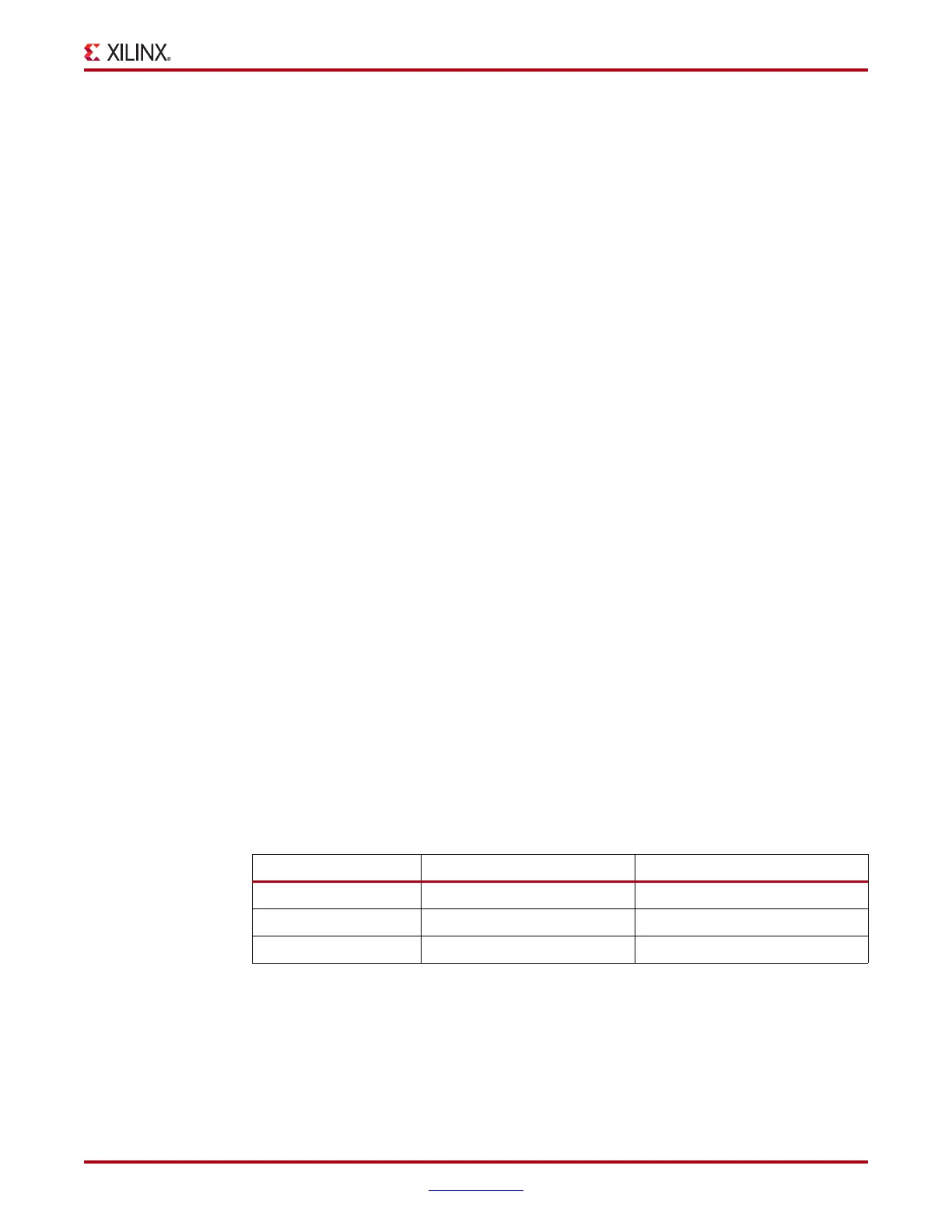
The PLL has a nominal operation range between 1.2 to 2.7 GHz for -1 speed grade devices
and 1.2 to 3.3 GHz for -2 and -3 speed -grade devices. Refer to the Virtex-6 FPGA Data Sheet
for the operating limits. The PLL output has a divider that can divide the output frequency
by one, two, or four. Table 2-6 shows the line rates typically supported by each divider
setting. An overlapping frequency range exists between PLL output divider settings. The
overlapping range provides flexibility with different PLL frequency options in multi-rate
applications.
Lower line rate support requires either fabric-based oversampling circuits or the built-in
5X oversampling block.
Table 2-6: Supported Line Rates per Divider Setting
PLL Output Divider -1 Line Rate Range (Gb/s) -2/-3 Line Rate Range (Gb/s)
1 2.4 to 5.0 2.4 to 6.6
2 1.2 to 2.7 1.2 to 3.3
4 0.6 to 1.35 0.6 to 1.65

 Loading...

