Virtex-6 FPGA GTX Transceivers User Guide www.xilinx.com 207
UG366 (v2.5) January 17, 2011
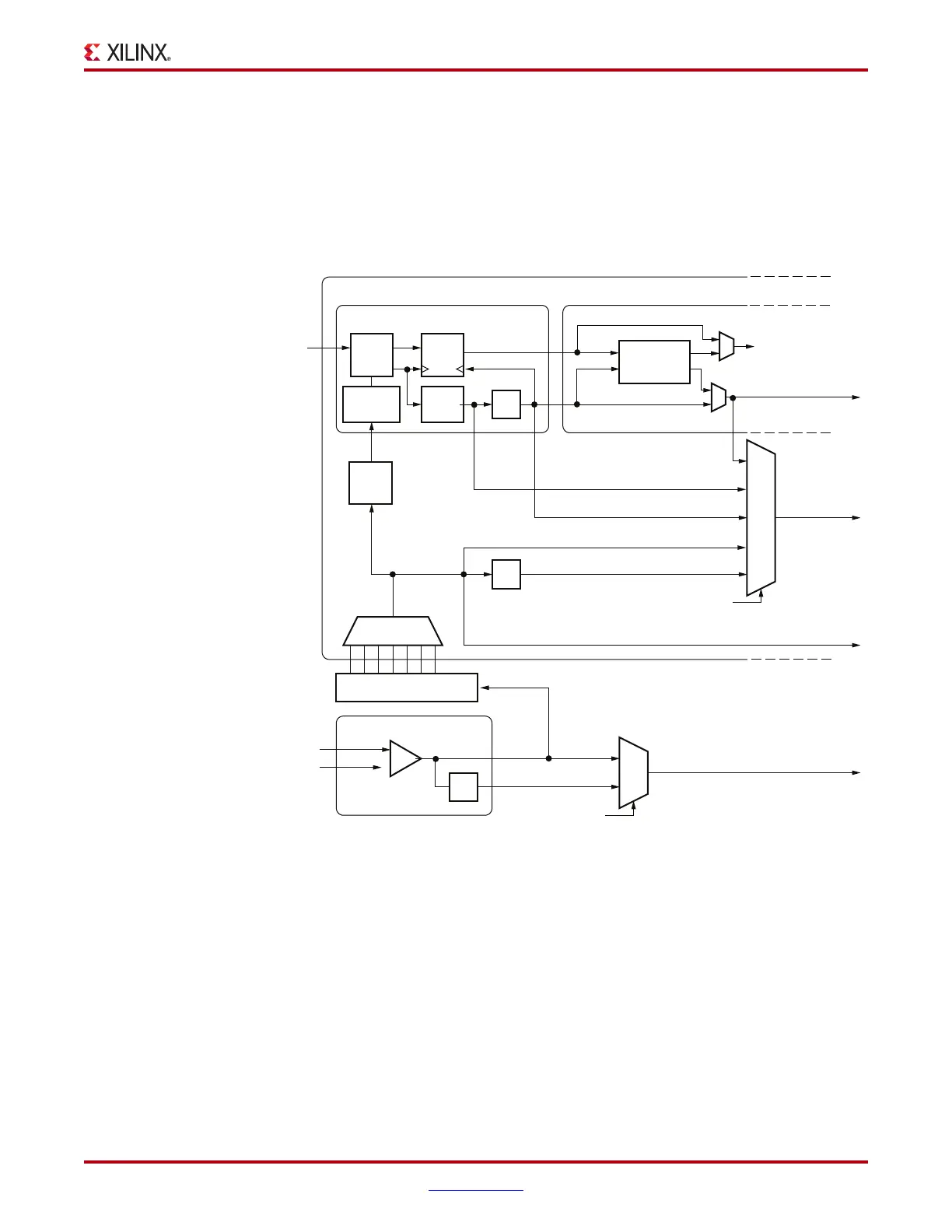
RX Fabric Clock Output Control
RX Fabric Clock Output Control
Functional Description
The RX Clock Divider Control block has two main components: serial clock divider control
and parallel clock divider and selector control. The clock divider and selector details are
illustrated in Figure 4-15.
Notes relevant to Figure 4-15:
1. RXRECCLKPCS and MGTREFCLKFAB[1] are redundant outputs. Use RXRECCLK for
new designs.
2. The REFCLK_CTRL option is controlled automatically by software and is not user
selectable. The user can only route one of IBUFDS_GTXE1’s O or ODIV2 outputs to the
fabric.
3. IBUFDS_GTXE1 is a redundant output for additional clocking scheme flexibility.
4. The selection of the /4 or /5 divider block is dependent on RX_DATA_WIDTH (see
Table 4-56, page 269):
• /4 is selected when the internal data width is 16
• /5 is selected when the internal data width is 20
X-Ref Target - Figure 4-15
Figure 4-15: RX Serial and Parallel Clock Divider Detail
UG366_c4_14_120809
RX PMA RX PCS
RXRECCLKPCS
RXRECCLK
000
001
010
011
100
RXDATA
RXRECCLKPCS
SIPO
REFCLK Distribution
0
1
O
REFCLK Sel
GTXE1 (GTX Transceiver Primitive)
RXP/N
CDR
RX Over-
sampler
RXDATA From
Downstream
PCS Blocks
/4 or
/5
/D
{1,2,4}
/2
RXRECCLKPMA_DIV1
RXRECCLKPMA_DIV2
RXPLLREFCLK_DIV1
RXPLLREFCLK_DIV2
RXRECCLK_CTRL (Attribute)
RX
PLL
MGTREFCLKFAB[1]
IBUFDS_GTXE1
Output to Fabric
IBUFDS_GTXE1
MGT
REFCLK
0/1
/2
ODIV2
REFCLK_CTRL
/2
O

 Loading...

