172 www.xilinx.com Virtex-6 FPGA GTX Transceivers User Guide
UG366 (v2.5) January 17, 2011
Chapter 3: Transmitter
After a PCI Express line rate change and if the TX buffer is bypassed, it is necessary to
perform a TX phase alignment and reset the TX PLL output clock divider. Refer to TX
Buffer Bypass, page 155 for more information on TX phase alignment.
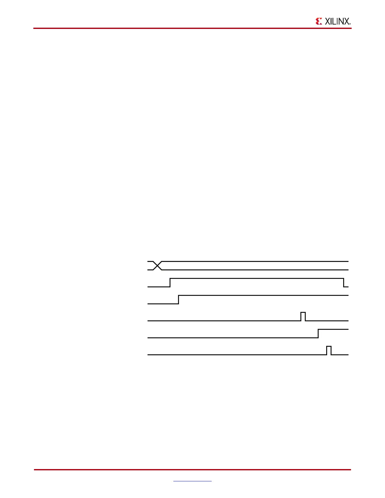
The rate change procedure for PCI Express 2.0 operation is:
1. Set TXPOWERDOWN[1:0] = 00.
2. Assert TXELECIDLE.
3. Set a new TXRATE[1:0] rate:
a. Tie TXRATE[1] = 1 in PCIe mode
b. Set TXRATE[0] = 0 (2.5 Gb/s line rate)
c. Set TXRATE[0] = 1 (5.0 Gb/s line rate)
4. Wait for the TXRATEDONE pulse.
5. Select a new TXUSRCLK2 or user clock frequency from BUFGMUX:
a. Select TXUSRCLK2 = 125 MHz (2.5 Gb/s line rate)
b. Select TXUSRCLK2 = 250 MHz (5.0 Gb/s line rate)
6. Wait for the PHYSTATUS pulse.
7. Deassert TXELECIDLE. TXELECIDLE can instead be deasserted after TX phase
alignment.
8. Perform TX phase alignment after the rate change (see TX Phase Alignment after Rate
Change Use Mode, page 159 for more information).
Figure 3-30 shows the rate change timing waveforms for PCI Express operation. In
Figure 3-30, TXRATE_SEL is a FPGA user logic control signal that selects a new
TXUSRCLK2 frequency (125 MHz or 250 MHz) from the BUFGMUX for a rate change.
TX Configurable Driver
Functional Description
The GTX TX driver is a high-speed current-mode differential output buffer. To maximize
signal integrity, it includes these features:
• Differential voltage control
X-Ref Target - Figure 3-30
Figure 3-30: Rate Change Timing for PCI Express Operation
TXPOWERDOWN
TXELECIDLE
TXRATE[0]
TXRATEDONE
TXRATESEL to
BUFGMUX
PHYSTAT US
from GTX
Line Rate = 5.0 Gb/s
TXUSRCLK2 = 125 MHz
Line Rate
= 2.5 Gb/s
TXUSRCLK2
= 250 MHz
00
UG366_c3_32_071009

 Loading...
