246 www.xilinx.com Virtex-6 FPGA GTX Transceivers User Guide
UG366 (v2.5) January 17, 2011
Chapter 4: Receiver
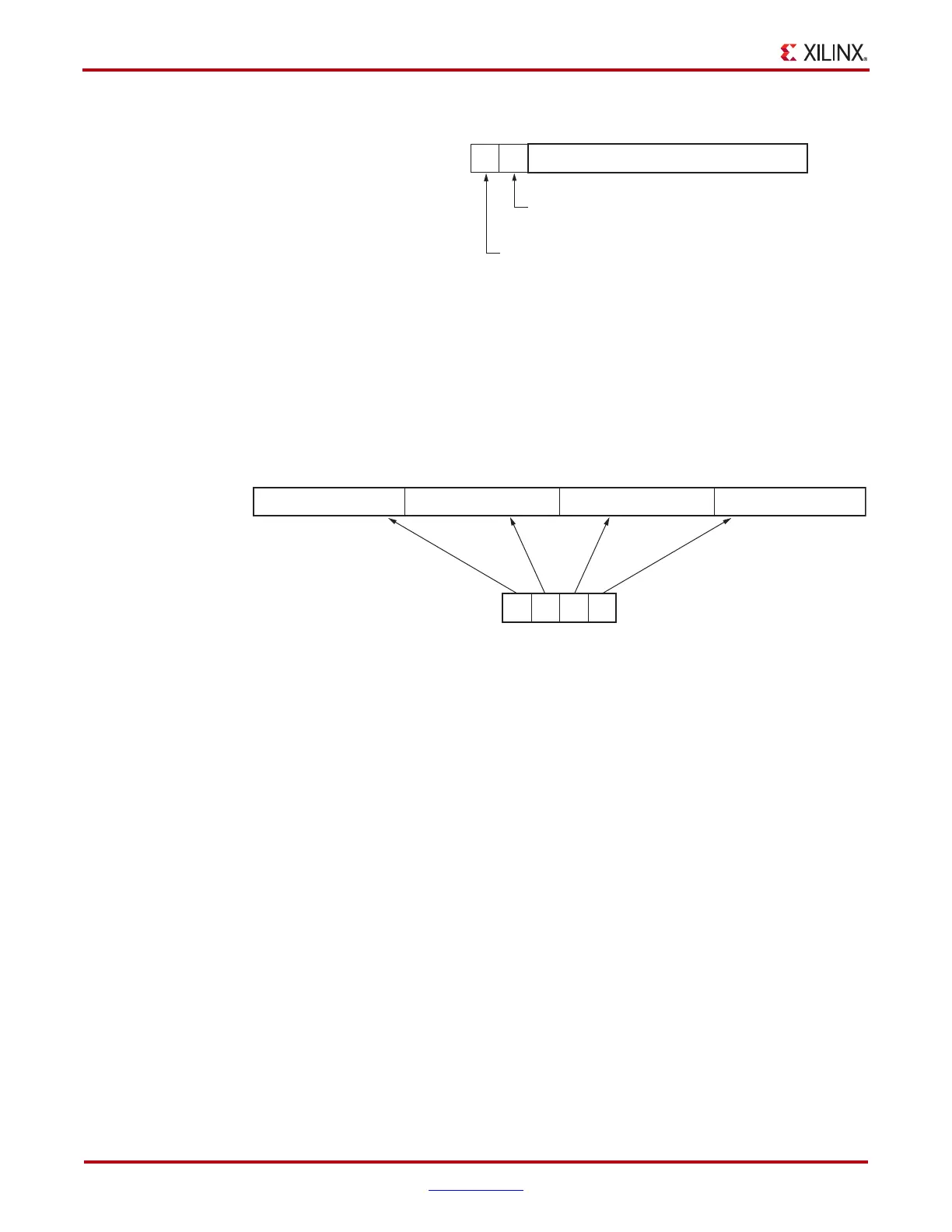
Some protocols use clock correction sequences with don’t care subsequences. The clock
correction circuit can be programmed to recognize these sequences using
CLK_COR_SEQ_1_ENABLE and CLK_COR_SEQ_2_ENABLE. When the enable bit for a
sequence is Low, that byte is considered matched no matter what the value. Figure 4-37
shows the mapping between the clock correction sequences and the clock correction
sequence enable bits.
Clock Correction Options
CLK_COR_REPEAT_WAIT is used to control the clock correction frequency. This value is
set to the minimum number of RXUSRCLK cycles required between clock correction
events. This attribute is set to 0 to allow clock correction to occur any time.
Some protocols allow clock correction to occur at any time, but require that if the clock
correction circuit removes sequences, at least one sequence stays in the stream. For
protocols with this requirement, CLK_COR_KEEP_IDLE is set to TRUE.
Monitoring Clock Correction
The clock correction circuit can be monitored using the RXCLKCORCNT and
RXBUFSTATUS ports. The RXCLKCORCNT entry in Table 4-46 shows how to decode the
values of RXCLKCORCNT to determine the status of the clock correction circuit. The
RXBUFSTATUS entry in Table 4-46 shows how to decode the values of RXBUFSTATUS to
determine how full the RX elastic buffer is.
In addition to RXCLKCORCNT and RXBUFSTATUS, RXRUNDISP can be taken from the
8B/10B decoder interface (see RX 8B/10B Decoder, page 228) and used to indicate when
RXDATA has the first byte of a clock correction sequence that was replicated and added to
the RX elastic buffer. To use the RXRUNDISP port to indicate inserted idles instead of the
current RX running disparity, CLK_COR_INSERT_IDLE_FLAG is set to TRUE.
X-Ref Target - Figure 4-36
Figure 4-36: Clock Correction Subsequence Settings with
RX_DECODE_SEQ_MATCH = TRUE
X-Ref Target - Figure 4-37
Figure 4-37: Clock Correction Sequence Mapping
8-Bit Clock Correction Sequence
1 = Sequence is a K Character
0 = Sequence is a Regular Character
1 = Sequence Uses Inverted Disparity
0 = Sequence Uses Regular Disparity
7:0
UG366_c4_33_051509
89CLK_COR_SEQ_x_y
UG366_c4_34_051509
3412
CLK_COR_SEQ_x_4 CLK_COR_SEQ_x_3 CLK_COR_SEQ_x_2
CLK_COR_SEQ_x_ENABLE
CLK_COR_SEQ_x_1

 Loading...

