Virtex-6 FPGA GTX Transceivers User Guide www.xilinx.com 287
UG366 (v2.5) January 17, 2011
Power Supply and Filtering
This subsection discusses some issues regarding the implementation of these design issues
on the PCB.
Board Stackup
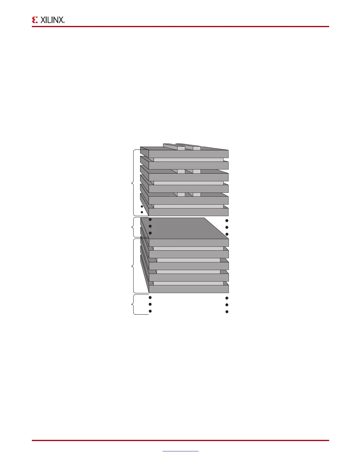
For Virtex-6 FPGA GTX transceivers, the board stackup layers can be grouped into power
distribution layers and signal routing layers. The power distribution layer group connects
the power supply sources for MGTAVCC and MGTAVTT to the power supply pins on the
Virtex-6 FPGA. Circuit board traces for receiver and transmitter data and the reference
clock are provided in the signal routing layer group. These two layer groups can be
considered separately within the stackup because it is the relative position of the layers
within each group that is important. Figure 5-11 shows how the groups can be
incorporated into an overall PCB stackup.
In this stackup, the GTX transceiver signal layers are at the top of the stackup. This group
is composed of three signal routing layers and three plane layers. The planes provide a
return current path for the transmission lines on the signal layers. Each of the signal
routing layers is shielded from adjacent layers by a ground plane. Because of this
shielding, the traces on each signal layer can be routed without having to consider the
routing on an adjacent layer. This increases the routing channels on each signal layer,
giving the layout designer more options for achieving an optimal signal breakout.
The GTX power layer group is treated as an autonomous group of layers that can be placed
within the overall board stackup. This group of layers consists of a layer for each of the
GTX power supplies (MGTAVCC and MGTAVTT) sandwiched between two ground
layers. The ground layers provide shielding to the power planes from signals routed on
X-Ref Target - Figure 5-11
Figure 5-11: Stackup for GTX Power and Signal Layers
Tranceiver
Signal
Layers
Layer 1 (Top - Signal Microstrip Routing)
Layer 2 (GND Plane)
Layer 3 (Signal Stripline Routing)
Layer 4 (GND Plane)
Layer 5 (Signal Stripline Routing)
Layer 6 (GND Plane)
Layer N (GND Plane)
Layer N+1 (MGTAVTT Power Island)
Layer N+2 (MGTAVCC Power Island)
Layer N+3 (GND Plane)
Other
Layers in
Board
Stackup
Other
Layers in
Board
Stackup
Tranceiver
Power
Layers
UG366_c5_11_051509

 Loading...

